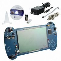
CY8CKIT-006 Cypress Semiconductor Corp, CY8CKIT-006 Datasheet - Page 28

CY8CKIT-006
Manufacturer Part Number
CY8CKIT-006
Description
KIT DEV PSOC3 LCD SEGMENT
Manufacturer
Cypress Semiconductor Corp
Series
PSOC™ 3r
Specifications of CY8CKIT-006
Main Purpose
Displays, LCD Display
Embedded
Yes, MCU, 32-Bit
Primary Attributes
448 addressable segments
Secondary Attributes
Configurable LCD pin selection
Description/function
Evaluation Kit
Interface Type
USB
Backlighting
No Backlighting
Data Bus Width
8 bit, 16 bit, 32 bit
Maximum Operating Temperature
+ 50 C
Minimum Operating Temperature
0 C
Number Of Segments
7
Operating Supply Voltage
12 V
Operating Voltage
3.3 V
Pixel Format
16 x 28
Product
Display Modules
Software
Software Included
Touch Panel
No Touch Panel
For Use With/related Products
PSoC 3
Lead Free Status / RoHS Status
Lead free / RoHS Compliant
Utilized Ic / Part
-
Lead Free Status / Rohs Status
Lead free / RoHS Compliant
Other names
428-2994
Available stocks
Company
Part Number
Manufacturer
Quantity
Price
Company:
Part Number:
CY8CKIT-006
Manufacturer:
Cypress Semiconductor Corp
Quantity:
135
Firmware
5.2.4
5.2.5
5.3
5.3.1
5.3.1.1
28
pled and displayed on alternating cycle with the date readings. Therefore, the date and temperature
automatically and continuously alternates on the display. The temperature display can be alternated
between °C and °F by pressing the "+" or "-".
Contrast Adjustments
To adjust the contrast dynamically, the project calls the adjust bias API call provided by the Segment
LCD component. The higher the bias level set in the call to the API the higher the contrast. The API
allows a selection between 0 and 127 with 127 corresponding to the maximum contrast level.
Enter a relative value between 0 and 10; the code maps the contrast setting into bias voltage values
within the range 47 to 67 (3.23V to 3.78V).
LCD Demonstration
To demonstrate all the segments of LCD glass, the project sequentially demonstrates the various
display sections. Refer to
LCD glass are displayed.
Project Design and Setup
Analog I/O
Thermistor Reference Voltage
The thermistor reference voltage analog connection is configured as an input but is actually an out-
put. The VDAC generates a fixed constant output voltage on the analog port. This reference voltage
is also sent through the AMUX to be sampled by the Delta-Sigma ADC during temperature calcula-
tion periods.
The output is configured for 1-pin width mapping and Hi-Z Analog during Power-On Reset. The port
pin is set for High Impedance Analog. The default Built-In settings are used.
Figure 5-4. Thermistor Reference Analog Port Configuration: General Tab
CY8CKIT-006 PSoC 3 LCD Segment Drive Evaluation Kit Guide, Doc. # 001-52798 Rev. *C
Figure 5-64
to know the details of sequence in which various sections of
[+] Feedback


