STEVAL-IFW001V1 STMicroelectronics, STEVAL-IFW001V1 Datasheet - Page 12
STEVAL-IFW001V1
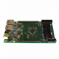
Manufacturer Part Number
STEVAL-IFW001V1
Description
BOARD EVAL BASED ON STR912FA
Manufacturer
STMicroelectronics
Datasheets
1.STEVAL-IFW001V1.pdf
(102 pages)
2.STEVAL-IFW001V1.pdf
(9 pages)
3.STEVAL-IFW001V1.pdf
(7 pages)
Specifications of STEVAL-IFW001V1
Design Resources
STEVAL-IFW001V1 Gerber Files STEVAL-IFW001V1 Schematic STEVAL-IFW001V1 Bill of Material
Main Purpose
Interface, Ethernet
Embedded
Yes, MCU, 32-Bit
Utilized Ic / Part
E-STE101P, STR912FAW44
Primary Attributes
Dual Ethernet Transceivers for Full Duplex Communication
Secondary Attributes
Up to 32 MII Addresses, UART, I2C, SPI, with RJ45 Connectors
Silicon Manufacturer
ST Micro
Core Architecture
ARM
Core Sub-architecture
ARM9
Silicon Core Number
STR9
Silicon Family Name
STR91x
For Use With
497-8263 - BOARD EXTENSION STEVAL-IFW001V1
Lead Free Status / RoHS Status
Lead free / RoHS Compliant
Other names
497-8262


Functional overview
3
3.1
3.2
3.3
3.4
3.4.1
12/102
Functional overview
System-in-a-package (SiP)
The STR91xFA is a SiP device, comprised of two stacked die. One die is the ARM966E-S
CPU with peripheral interfaces and analog functions, and the other die is the burst Flash.
The two die are connected to each other by a custom high-speed 32-bit burst memory
interface and a serial JTAG test/programming interface.
Package choice
STR91xFA devices are available in 128-pin (14 x 14 mm) and 80-pin (12 x 12 mm) LQFP
and LFBGA144 (10 x 10 mm) packages. Refer to
list of available peripherals for each of the package choices.
ARM966E-S CPU core
The ARM966E-S core inherently has separate instruction and data memory interfaces
(Harvard architecture), allowing the CPU to simultaneously fetch an instruction, and read or
write a data item through two Tightly-Coupled Memory (TCM) interfaces as shown in
Figure
reduction in cycle count per instruction. In addition to this, a 5-stage pipeline is used to
increase the amount of operational parallelism, giving the most performance out of each
clock cycle.
Ten DSP-enhanced instruction extensions are supported by this core, including single-cycle
execution of 32x16 Multiply-Accumulate, saturating addition/subtraction, and count leading-
zeros.
The ARM966E-S core is binary compatible with 32-bit ARM7 code and 16-bit Thumb
Burst Flash memory interface
A burst Flash memory interface
(I-TCM) path of the ARM966E-S core. Also in this path is an 8-instruction Pre-Fetch Queue
(PFQ) and a 15-entry Branch Cache (BC), enabling the ARM966E-S core to perform up to
96 MIPS while executing code directly from Flash memory. This architecture provides high
performance levels without a costly instruction SRAM, instruction cache, or external
SDRAM. Eliminating the instruction cache also means interrupt latency is reduced and code
execution becomes more deterministic.
Pre-fetch queue (PFQ)
As the CPU core accesses sequential instructions through the I-TCM, the PFQ always looks
ahead and will pre-fetch instructions, taking advantage any idle bus cycles due to variable
length instructions. The PFQ will fetch 32-bits at a time from the burst Flash memory at a
rate of up to 96 MHz.
1. The result is streamlined CPU Load and Store operations and a significant
Doc ID 13495 Rev 6
(Figure
1) has been integrated into the Instruction TCM
Table 2: Device summary on page 11
STR91xFAxxx
®
code.
for a
Related parts for STEVAL-IFW001V1
Image
Part Number
Description
Manufacturer
Datasheet
Request
R

Part Number:
Description:
BOARD EVAL SPZB260 MOD FOR STR9
Manufacturer:
STMicroelectronics
Datasheet:

Part Number:
Description:
BOARD EVAL EXTENSION SN250
Manufacturer:
STMicroelectronics
Datasheet:

Part Number:
Description:
BOARD EVAL AB-54003L-512
Manufacturer:
STMicroelectronics
Datasheet:

Part Number:
Description:
BOARD REF DESIGN RF DMOS PWR AMP
Manufacturer:
STMicroelectronics
Datasheet:

Part Number:
Description:
BOARD EVAL PWR AMP AB-84008L-470
Manufacturer:
STMicroelectronics
Datasheet:

Part Number:
Description:
BOARD EVAL FOR STM32F103XX
Manufacturer:
STMicroelectronics
Datasheet:

Part Number:
Description:
BOARD EVAL AB-54003L-512
Manufacturer:
STMicroelectronics
Datasheet:

Part Number:
Description:
BOARD SMART PLUG STM32 SPZB260PR
Manufacturer:
STMicroelectronics
Datasheet:

Part Number:
Description:
BOARD DEMO BLUETOOTH SPBT2532C2
Manufacturer:
STMicroelectronics
Datasheet:
Part Number:
Description:
ZIGBEE USB DONGLE EVAL KIT
Manufacturer:
STMicroelectronics
Datasheet:
Part Number:
Description:
STMicroelectronics [RIPPLE-CARRY BINARY COUNTER/DIVIDERS]
Manufacturer:
STMicroelectronics
Datasheet:
Part Number:
Description:
STMicroelectronics [LIQUID-CRYSTAL DISPLAY DRIVERS]
Manufacturer:
STMicroelectronics
Datasheet:

Part Number:
Description:
BOARD EVAL FOR MEMS SENSORS
Manufacturer:
STMicroelectronics
Datasheet: