NCP1605FORWGEVB ON Semiconductor, NCP1605FORWGEVB Datasheet - Page 14
NCP1605FORWGEVB
Manufacturer Part Number
NCP1605FORWGEVB
Description
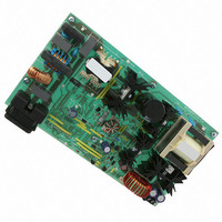
EVAL BOARD FOR NCP1605FORWG
Manufacturer
ON Semiconductor
Datasheets
1.NCP1217P100G.pdf
(19 pages)
2.NCP1605ADR2G.pdf
(32 pages)
3.NCP1605FORWGEVB.pdf
(2 pages)
4.NCP1605FORWGEVB.pdf
(20 pages)
Specifications of NCP1605FORWGEVB
Design Resources
NCP1605FORWGEVB BOM NCP1605FORWGEVB Gerber Files NCP1605 EVB Schematic
Main Purpose
AC/DC, Primary and Secondary Side with PFC
Outputs And Type
1, Isolated
Voltage - Output
19V
Current - Output
8A
Voltage - Input
90 ~ 265VAC
Regulator Topology
Forward Converter
Frequency - Switching
133kHz
Board Type
Fully Populated
Utilized Ic / Part
NCP1217, NCP1605
Lead Free Status / RoHS Status
Lead free / RoHS Compliant
Power - Output
-
Lead Free Status / Rohs Status
Lead free / RoHS Compliant
For Use With/related Products
NCP1605FORWG
Other names
NCP1605FORWGEVBOS


415
405
395
385
375
365
355
345
335
325
108
106
104
220
200
180
160
140
120
100
112
110
80
60
40
−40
−40
−40
Figure 44. Ratio (I
Figure 46. Delay from (ZCD Pin Low) to
−15
−15
−15
Figure 42. Pin 7 Source Current @
T
T
T
V
J
J
J
(DRV High) vs. Temperature
, JUNCTION TEMPERATURE (°C)
, JUNCTION TEMPERATURE (°C)
, JUNCTION TEMPERATURE (°C)
PIN4
10
10
10
= 2.5 V vs. Temperature
Temperature
PIN6
35
35
35
/ I
PIN5
60
) @ I
60
60
PIN5
85
85
85
= 10 mA vs.
http://onsemi.com
110
110
110
14
340
330
320
310
300
290
280
270
260
200
180
160
140
120
100
80
60
40
8
7
6
5
4
3
−40
−40
−40
(Pin 7 Charge Current) that is (V
Figure 45. Pin 6 Comparator Threshold vs.
Figure 43. Ratio Pin 7 Clamp Voltage /
−15
−15
−15
@ V
Figure 47. Skip Cycle Threshold
T
T
T
(V
J
J
J
, JUNCTION TEMPERATURE (°C)
, JUNCTION TEMPERATURE (°C)
, JUNCTION TEMPERATURE (°C)
PIN1
PIN6
10
10
10
Falling) vs. Temperature
= 0 V and V
Temperature
35
35
35
PIN4
60
60
60
= 1.75 V
CLCRM
85
85
85
/ I
RAMP
110
110
110
)
Related parts for NCP1605FORWGEVB
Image
Part Number
Description
Manufacturer
Datasheet
Request
R

Part Number:
Description:
ON Semiconductor [VOLTAGE REGULATOR]
Manufacturer:
ON Semiconductor
Datasheet:
Part Number:
Description:
357-036-542-201 CARDEDGE 36POS DL .156 BLK LOPRO
Manufacturer:
ON Semiconductor
Datasheet:
Part Number:
Description:
357-036-542-201 CARDEDGE 36POS DL .156 BLK LOPRO
Manufacturer:
ON Semiconductor
Datasheet:
Part Number:
Description:
357-036-542-201 CARDEDGE 36POS DL .156 BLK LOPRO
Manufacturer:
ON Semiconductor
Datasheet:
Part Number:
Description:
357-036-542-201 CARDEDGE 36POS DL .156 BLK LOPRO
Manufacturer:
ON Semiconductor
Datasheet:
Part Number:
Description:
357-036-542-201 CARDEDGE 36POS DL .156 BLK LOPRO
Manufacturer:
ON Semiconductor
Datasheet:
Part Number:
Description:
357-036-542-201 CARDEDGE 36POS DL .156 BLK LOPRO
Manufacturer:
ON Semiconductor
Datasheet:
Part Number:
Description:
357-036-542-201 CARDEDGE 36POS DL .156 BLK LOPRO
Manufacturer:
ON Semiconductor
Datasheet:
Part Number:
Description:
357-036-542-201 CARDEDGE 36POS DL .156 BLK LOPRO
Manufacturer:
ON Semiconductor
Datasheet:
Part Number:
Description:
357-036-542-201 CARDEDGE 36POS DL .156 BLK LOPRO
Manufacturer:
ON Semiconductor
Datasheet:
Part Number:
Description:
357-036-542-201 CARDEDGE 36POS DL .156 BLK LOPRO
Manufacturer:
ON Semiconductor
Datasheet:
Part Number:
Description:
Manufacturer:
ON Semiconductor
Datasheet:
Part Number:
Description:
Manufacturer:
ON Semiconductor
Datasheet:
Part Number:
Description:
Manufacturer:
ON Semiconductor
Datasheet: