NCP1605FORWGEVB ON Semiconductor, NCP1605FORWGEVB Datasheet - Page 25
NCP1605FORWGEVB
Manufacturer Part Number
NCP1605FORWGEVB
Description
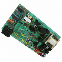
EVAL BOARD FOR NCP1605FORWG
Manufacturer
ON Semiconductor
Datasheets
1.NCP1217P100G.pdf
(19 pages)
2.NCP1605ADR2G.pdf
(32 pages)
3.NCP1605FORWGEVB.pdf
(2 pages)
4.NCP1605FORWGEVB.pdf
(20 pages)
Specifications of NCP1605FORWGEVB
Design Resources
NCP1605FORWGEVB BOM NCP1605FORWGEVB Gerber Files NCP1605 EVB Schematic
Main Purpose
AC/DC, Primary and Secondary Side with PFC
Outputs And Type
1, Isolated
Voltage - Output
19V
Current - Output
8A
Voltage - Input
90 ~ 265VAC
Regulator Topology
Forward Converter
Frequency - Switching
133kHz
Board Type
Fully Populated
Utilized Ic / Part
NCP1217, NCP1605
Lead Free Status / RoHS Status
Lead free / RoHS Compliant
Power - Output
-
Lead Free Status / Rohs Status
Lead free / RoHS Compliant
For Use With/related Products
NCP1605FORWG
Other names
NCP1605FORWGEVBOS


Remark:
•
•
•
Oscillator / Synchronization Section
latch and turn the MOSFET on. The oscillator frequency is
set by the capacitor that is applied to Pin 8. Typically,
820 pF force about 60 kHz. The maximum allowable
oscillator frequency is 250 kHz. The clock frequency can
also be driven by an external synchronization signal.
This block contains two main parts (refer to Figure 66):
•
V
The oscillator generates the clock signal to set the PWM
CONTROL
Skip cycle is not allowed during the PFC startup phase
to avoid that it interferes with the soft−start. That is why,
skip cycle is enabled only when “pfcOK” is high.
Each working phase of the burst mode starts smoothly as
Pin 3 is grounded at the beginning of it. This soft−start
capability is effective to avoid the audible noise that
could possibly result from such a burst operation.
The circuit leaves the standby mode when the output
voltage goes below 95.5% of its regulation level and
V
The arrangement that consists of charging/discharging
current sources, a switch and a comparator. When used
in oscillator mode, a capacitor is connected between
Pin 8 and ground. A current source (100 mA) charges the
Pin 8 capacitor until its voltage exceeds VoscH. At that
moment, the comparator (“COMP_OSC”) turns high and
activates the discharge current source (200 mA). As a
consequence, Pin 8 actually sinks 100 mA that discharge
the oscillator capacitor to VoscL. At that moment, the
comparator turns low and initiates a new charge phase. If
the circuit is to be externally triggered, the
synchronization signal must cross VoscL and VoscH to
V
V
V
SKIP
Drive
Pin1
OUT
OUT
Pin1
L
is above 330 mV (300 mV + 30 mV hysteresis).
Figure 64. Standby Management
http://onsemi.com
25
•
switching frequency.
end of a clock period and the circuit would enter Continuous
Conduction Mode (CCM) if the MOSFET turned on in that
moment. In order to prevent CCM, the “storing circuitry” of
the oscillator / synchronization block, memorizes the
“COMP_OSC” rising edge (thanks to the “CLOCK
Generation” latch) and delays the next MOSFET conduction
time until the coil current has totally vanished (that is until the
signal “DT” is high − “DT” is generated by the current sense
block so that it is high during the dead−time and low
otherwise). In other words, CRM operation is obtained (refer
to Figure 65).
The oscillator / Synchronization block is designed to set the
However, the coil current can possibly be non zero at the
properly turn on and off the “COMP_OSC” comparator.
Also the synchronization signal must be low impedance
enough not to be distorted by the Pin 8 source and sink
currents.
The “storing circuitry” that contains a latch and some
gates. The raising edge of the “COMP_OSC” output sets
the “CLOCK Generation” latch to turn high the “CLK”
signal. If the timing capacitor of Pin 7 is properly
discharged (V
PWM block is ready for a new cycle and “CLK” can
force the signal “V
the PWM latch sets. In addition, “V
“CLOCK Generation” latch to make it ready for the next
oscillator cycle. The two inverters of Figure 66, simply
generate some delay to ensure that “V
long enough to set the PWM latch and reset the
“CLOCK Generation” latch (longer delay than that
produced by the two gates, may actually be necessary).
Pin4
95.5% of the Regulation Level
<50 mV leading to “C
SET
” in high state. As a consequence,
300 mV
SET
SET
” resets the
T
OK” high), the
” keeps high
Related parts for NCP1605FORWGEVB
Image
Part Number
Description
Manufacturer
Datasheet
Request
R

Part Number:
Description:
ON Semiconductor [VOLTAGE REGULATOR]
Manufacturer:
ON Semiconductor
Datasheet:
Part Number:
Description:
357-036-542-201 CARDEDGE 36POS DL .156 BLK LOPRO
Manufacturer:
ON Semiconductor
Datasheet:
Part Number:
Description:
357-036-542-201 CARDEDGE 36POS DL .156 BLK LOPRO
Manufacturer:
ON Semiconductor
Datasheet:
Part Number:
Description:
357-036-542-201 CARDEDGE 36POS DL .156 BLK LOPRO
Manufacturer:
ON Semiconductor
Datasheet:
Part Number:
Description:
357-036-542-201 CARDEDGE 36POS DL .156 BLK LOPRO
Manufacturer:
ON Semiconductor
Datasheet:
Part Number:
Description:
357-036-542-201 CARDEDGE 36POS DL .156 BLK LOPRO
Manufacturer:
ON Semiconductor
Datasheet:
Part Number:
Description:
357-036-542-201 CARDEDGE 36POS DL .156 BLK LOPRO
Manufacturer:
ON Semiconductor
Datasheet:
Part Number:
Description:
357-036-542-201 CARDEDGE 36POS DL .156 BLK LOPRO
Manufacturer:
ON Semiconductor
Datasheet:
Part Number:
Description:
357-036-542-201 CARDEDGE 36POS DL .156 BLK LOPRO
Manufacturer:
ON Semiconductor
Datasheet:
Part Number:
Description:
357-036-542-201 CARDEDGE 36POS DL .156 BLK LOPRO
Manufacturer:
ON Semiconductor
Datasheet:
Part Number:
Description:
357-036-542-201 CARDEDGE 36POS DL .156 BLK LOPRO
Manufacturer:
ON Semiconductor
Datasheet:
Part Number:
Description:
Manufacturer:
ON Semiconductor
Datasheet:
Part Number:
Description:
Manufacturer:
ON Semiconductor
Datasheet:
Part Number:
Description:
Manufacturer:
ON Semiconductor
Datasheet: