NCP1605FORWGEVB ON Semiconductor, NCP1605FORWGEVB Datasheet - Page 4
NCP1605FORWGEVB
Manufacturer Part Number
NCP1605FORWGEVB
Description
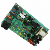
EVAL BOARD FOR NCP1605FORWG
Manufacturer
ON Semiconductor
Datasheets
1.NCP1217P100G.pdf
(19 pages)
2.NCP1605ADR2G.pdf
(32 pages)
3.NCP1605FORWGEVB.pdf
(2 pages)
4.NCP1605FORWGEVB.pdf
(20 pages)
Specifications of NCP1605FORWGEVB
Design Resources
NCP1605FORWGEVB BOM NCP1605FORWGEVB Gerber Files NCP1605 EVB Schematic
Main Purpose
AC/DC, Primary and Secondary Side with PFC
Outputs And Type
1, Isolated
Voltage - Output
19V
Current - Output
8A
Voltage - Input
90 ~ 265VAC
Regulator Topology
Forward Converter
Frequency - Switching
133kHz
Board Type
Fully Populated
Utilized Ic / Part
NCP1217, NCP1605
Lead Free Status / RoHS Status
Lead free / RoHS Compliant
Power - Output
-
Lead Free Status / Rohs Status
Lead free / RoHS Compliant
For Use With/related Products
NCP1605FORWG
Other names
NCP1605FORWGEVBOS


Current Sense Block
Standby Input
Oscillator / Synchronization Block
pfcOK / REF5V
Brown−Out Detection Block
Thermal Shutdown
V
V
TYPICAL ELECTRICAL CHARACTERISTICS
(Conditions: V
3. Not tested; guaranteed by characterization
4. Not tested; guaranteed by design
CC
SKIP
I
RAMP_SINK
UNDERVOLTAGE Lockout Section
T
Symbol
V
Icap_ref
V
V
V
V
K
OUT
Off100
sync_min
H
H
K
V
I
Swing
T
Off10
T
pfcOK
V
V
V
T
charge
I
V
C
I
sync_H
pfcOK
IB
sync_L
CC
CS200
disch
MAX
LIMIT
TEMP
CS10
STBY
STBY
OCP
ZCD
BOH
INIT
ZCD
BOL
INT
BO
ON
/
H
L
V
OUT
CC
L Ratio (Pin 4 Voltage to terminate a SKIP period) over the
= 16 V, V
Average Pin 7 Internal Capacitance (V
Guaranteed by design
Maximum Pin 7 Voltage Allowing the Setting of the PWM Latch
Pin 7 Sink Current (Drive low) @ V
Current Sense Pin Voltage, 100 mA being drawn from Pin 5
Current Sense Pin Voltage, 10 mA being drawn from Pin 5
Overcurrent Protection Threshold
(Ipin5 > 250 mA) to (DRV low) Propagation Delay (Note 3)
Ratio (I
Ratio (I
Pin 6 Comparator Threshold
Delay from (V
Standby Mode Threshold (V
Hysteresis for Standby Mode Detection
(V
Oscillator Charge Current
Oscillator Discharge Current
Comparator Upper Threshold
Comparator Lower Threshold
Comparator Swing (V
Minimum Synchronization Pulse Width for Detection
Pin 12 Voltage @ V
Pin 12 Voltage @ V
with a 250 mA sourced by Pin 12
Pin 12 Voltage @ V
with a 5 mA sourced by Pin 12
Current Capability
Brown−Out Comparator Threshold (V
Brown−Out Comparator Threshold (V
Pin 2 Bias Current @ V
Thermal Shutdown Threshold
Thermal Shutdown Hysteresis
Turn on Threshold Level, V
OUT
HV
Low Detect Threshold) (Note 4)
Pin6
Pin6
= 50 V, V
/I
/I
Pin5
Pin5
Pin6
) @ I
) @ I
Pin2
< V
Pin13
Pin13
Pin13
Pin5
Pin5
ZCD
sync_H
= 2 V, V
Pin2
= 5 V, 250 mA being sunk by Pin 12
= 0 V and V
= 0 V and V
= 10 mA
= 200 mA
) to (DRV high)
CC
= 0.5 V and 1 V
Pin1
− V
Raising Up
Pin13
sync_L
falling)
Rating
Pin7
= 0 V, T
Pin3
Pin3
Pin2
Pin2
)
http://onsemi.com
Pin7
= 1 V
= 5 V,
= 5 V,
rising)
falling)
varying from 0 and 1 V)
J
from 0°C to +125°C, unless otherwise specified) (Note 2)
4
NCP1605A
NCP1605
−500
0.45
Min
−20
230
280
5 .0
3.0
0.9
4.7
4.5
0.9
9.5
99
98
50
25
99
90
90
14
−
−
−
−
−
−
−
−
−
−
−
0.50
10.5
Typ
250
100
108
101
100
120
310
100
100
100
155
8.0
3.0
2.0
1.0
5.0
5.0
1.0
15
50
10
30
60
10
15
15
0
−
−
Max
0.55
11.5
265
200
117
103
200
240
340
101
110
110
500
120
500
1.1
5.3
5.3
1.1
25
90
20
13
50
16
−
−
−
−
−
−
Unit
mV
mA
mV
mV
mV
mV
mV
mV
mA
mA
mA
mA
nA
pF
ns
ns
ns
°C
°C
%
%
%
V
V
V
V
V
V
V
Related parts for NCP1605FORWGEVB
Image
Part Number
Description
Manufacturer
Datasheet
Request
R

Part Number:
Description:
ON Semiconductor [VOLTAGE REGULATOR]
Manufacturer:
ON Semiconductor
Datasheet:
Part Number:
Description:
357-036-542-201 CARDEDGE 36POS DL .156 BLK LOPRO
Manufacturer:
ON Semiconductor
Datasheet:
Part Number:
Description:
357-036-542-201 CARDEDGE 36POS DL .156 BLK LOPRO
Manufacturer:
ON Semiconductor
Datasheet:
Part Number:
Description:
357-036-542-201 CARDEDGE 36POS DL .156 BLK LOPRO
Manufacturer:
ON Semiconductor
Datasheet:
Part Number:
Description:
357-036-542-201 CARDEDGE 36POS DL .156 BLK LOPRO
Manufacturer:
ON Semiconductor
Datasheet:
Part Number:
Description:
357-036-542-201 CARDEDGE 36POS DL .156 BLK LOPRO
Manufacturer:
ON Semiconductor
Datasheet:
Part Number:
Description:
357-036-542-201 CARDEDGE 36POS DL .156 BLK LOPRO
Manufacturer:
ON Semiconductor
Datasheet:
Part Number:
Description:
357-036-542-201 CARDEDGE 36POS DL .156 BLK LOPRO
Manufacturer:
ON Semiconductor
Datasheet:
Part Number:
Description:
357-036-542-201 CARDEDGE 36POS DL .156 BLK LOPRO
Manufacturer:
ON Semiconductor
Datasheet:
Part Number:
Description:
357-036-542-201 CARDEDGE 36POS DL .156 BLK LOPRO
Manufacturer:
ON Semiconductor
Datasheet:
Part Number:
Description:
357-036-542-201 CARDEDGE 36POS DL .156 BLK LOPRO
Manufacturer:
ON Semiconductor
Datasheet:
Part Number:
Description:
Manufacturer:
ON Semiconductor
Datasheet:
Part Number:
Description:
Manufacturer:
ON Semiconductor
Datasheet:
Part Number:
Description:
Manufacturer:
ON Semiconductor
Datasheet: