NCP1605FORWGEVB ON Semiconductor, NCP1605FORWGEVB Datasheet - Page 21
NCP1605FORWGEVB
Manufacturer Part Number
NCP1605FORWGEVB
Description
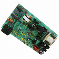
EVAL BOARD FOR NCP1605FORWG
Manufacturer
ON Semiconductor
Datasheets
1.NCP1217P100G.pdf
(19 pages)
2.NCP1605ADR2G.pdf
(32 pages)
3.NCP1605FORWGEVB.pdf
(2 pages)
4.NCP1605FORWGEVB.pdf
(20 pages)
Specifications of NCP1605FORWGEVB
Design Resources
NCP1605FORWGEVB BOM NCP1605FORWGEVB Gerber Files NCP1605 EVB Schematic
Main Purpose
AC/DC, Primary and Secondary Side with PFC
Outputs And Type
1, Isolated
Voltage - Output
19V
Current - Output
8A
Voltage - Input
90 ~ 265VAC
Regulator Topology
Forward Converter
Frequency - Switching
133kHz
Board Type
Fully Populated
Utilized Ic / Part
NCP1217, NCP1605
Lead Free Status / RoHS Status
Lead free / RoHS Compliant
Power - Output
-
Lead Free Status / Rohs Status
Lead free / RoHS Compliant
For Use With/related Products
NCP1605FORWG
Other names
NCP1605FORWGEVBOS


“pfcOK” signal of the block diagram, is high). This is
because, at the beginning of operation, the Pin 3 capacitor
must charge slowly and gradually for a soft−startup.
undershoots limitation is disabled as long as Pin 3 detects
standby conditions (V
risk of audible noise in standby thanks to the soft–start that
softens the bursts.
On−Time Control for Maximum Power Adjustment
amplifier output voltage to form a signal (V
by the PWM section to control the on−time. (V
compensates the relative weight of the dead−time sequences
measured during the precedent current cycles. During the
conduction time of the MOSFET, Pin 7 sources a current that
is proportional to the square of the voltage applied to Pin 4
(feedback pin). Practically, as Pin 4 receives a portion of the
output voltage (V
V
V
and voltage, respectively, t
switching period. Hence, the instantaneous input power is
given by the following equation:
where V
block. Hence, the average input power is:
The maximum value of V
power that can be delivered is:
power capability is inversely proportional to the square of the
output voltage. One sees that if the power demand is too high
to keep the regulation, (V
depends on the output voltage level that stabilizes to the
following value:
Where:
•
•
OUT
TON
Remark: As shown in block diagram, the circuitry for
As aforementioned, the NCP1605(A) processes the error
The MOSFET turns off when the Pin 7 voltage exceeds
The coil current averaged over one switching period is:
Where I
As aforementioned, we have: V
To the light of the last equations, one can note that the PFC
P IN (t) + V IN (t)I IN (t) +
P
And h is the efficiency.
OUT
.
. Hence, the MOSFET on−time (t1) is given by:
t 1 +
is the output power.
t I COIL u T + I IN (t) +
REGUL
IN
t P IN u MAX +
t P IN u+
(t) and V
V OUT +
C pin7 V TON
k V OUT
is the signal outputted by the regulation
OUT
IN
), I
Pin3
(t) are the instantaneous input current
2
2 L k V OUT
Pin7
C pin7 V ac
REGUL
< 300 mV). This is to suppress the
2
2 L k V OUT
REGUL
C pin7 V IN
2 L k h P OUT
is the core reset time and T is the
where k is a constant.
C pin7 1 V
is proportional to the square of
2 L k V OUT
C pin7 V ac
=1V) and the power delivery
TON
being 1 V, the maximum
V IN t 1
2
2
2 L
2
V REGUL
2
(t
@
1
V TON (t 1 ) t 2 )
+ t
(t 1 ) t 2 )
2
V ac
2
TON
2
1 V
T
)/T = V
) that is used
T
http://onsemi.com
REGUL
TON
)
21
“Follower Boost” is an operation mode where the
pre−converter output voltage stabilizes at a level that varies
linearly versus the ac line amplitude. This technique aims at
reducing the gap between the output and input voltages to
optimize the boost efficiency and minimize the cost of the
PFC stage (refer to the MC33260 data sheet for more
information, at:
http://www.onsemi.com/pub/Collateral/MC33260−D.PDF
discharged and maintained grounded when the drive is low.
Furthermore, the circuit compares the Pin 7 voltage to an
internal reference 50 mV and prevents the PWM latch from
being set as long as V
This is to guarantee that the timing capacitor is properly
discharged before starting a new cycle.
Current Sense and Zero Current Detection
voltage proportional to the coil current. Practically, a
current sense resistor (R
generate a negative voltage proportional to the coil current
(V
limitation of the maximum coil current and the detection
of the core reset (coil demagnetization). To do so, the
circuit incorporates an operational amplifier that sources
the current necessary to maintain the CS pin voltage null
(refer to Figure 60). By inserting a resistor R
the CS pin and R
Which leads to:
current.
•
•
Hence, one obtains the Follower Boost characteristics. The
Remark: the timing capacitor applied to Pin 7 is
The NCP1605(A) is designed to monitor a negative
In other words, the Pin 5 current is proportional to the coil
I
the coil current threshold for zero current detection is:
CS
If I
the PWM latch is reset. Hence, the maximum coil
current is:
The propagation delay (Ipin5 higher than 250 mA) to
(drive output low) is in the range of 100 ns, typically.
The Pin 5 current is internally copied and sourced by
Pin 6. Place a resistor (R
to build a voltage proportional to the coil current. The
circuit detects the core reset when V
100 mV, typically. The Pin 6 voltage equating:
Pin5
). The circuit uses V
Pin5
* [R CS I COIL ] ) [R OCP I pin5 ] + V pin5 [ 0
is utilized as follows:
exceeds 250 mA, an overcurrent is detected and
(I COIL )max +
V pin6 +
CS
I pin5 +
, we adjust the CS pin current as follows:
Pin7
R pin6 @ R cs
CS
) is inserted in the return path to
is higher than this low threshold.
R OCP
Pin6
R CS
R cs
R OCP
CS
) between Pin 6 and ground
R CS
for two functions: the
I COIL
@ I COIL ,
250 mA
Pin6
drops below
OCP
between
).
Related parts for NCP1605FORWGEVB
Image
Part Number
Description
Manufacturer
Datasheet
Request
R

Part Number:
Description:
ON Semiconductor [VOLTAGE REGULATOR]
Manufacturer:
ON Semiconductor
Datasheet:
Part Number:
Description:
357-036-542-201 CARDEDGE 36POS DL .156 BLK LOPRO
Manufacturer:
ON Semiconductor
Datasheet:
Part Number:
Description:
357-036-542-201 CARDEDGE 36POS DL .156 BLK LOPRO
Manufacturer:
ON Semiconductor
Datasheet:
Part Number:
Description:
357-036-542-201 CARDEDGE 36POS DL .156 BLK LOPRO
Manufacturer:
ON Semiconductor
Datasheet:
Part Number:
Description:
357-036-542-201 CARDEDGE 36POS DL .156 BLK LOPRO
Manufacturer:
ON Semiconductor
Datasheet:
Part Number:
Description:
357-036-542-201 CARDEDGE 36POS DL .156 BLK LOPRO
Manufacturer:
ON Semiconductor
Datasheet:
Part Number:
Description:
357-036-542-201 CARDEDGE 36POS DL .156 BLK LOPRO
Manufacturer:
ON Semiconductor
Datasheet:
Part Number:
Description:
357-036-542-201 CARDEDGE 36POS DL .156 BLK LOPRO
Manufacturer:
ON Semiconductor
Datasheet:
Part Number:
Description:
357-036-542-201 CARDEDGE 36POS DL .156 BLK LOPRO
Manufacturer:
ON Semiconductor
Datasheet:
Part Number:
Description:
357-036-542-201 CARDEDGE 36POS DL .156 BLK LOPRO
Manufacturer:
ON Semiconductor
Datasheet:
Part Number:
Description:
357-036-542-201 CARDEDGE 36POS DL .156 BLK LOPRO
Manufacturer:
ON Semiconductor
Datasheet:
Part Number:
Description:
Manufacturer:
ON Semiconductor
Datasheet:
Part Number:
Description:
Manufacturer:
ON Semiconductor
Datasheet:
Part Number:
Description:
Manufacturer:
ON Semiconductor
Datasheet: