NCP1605FORWGEVB ON Semiconductor, NCP1605FORWGEVB Datasheet - Page 27
NCP1605FORWGEVB
Manufacturer Part Number
NCP1605FORWGEVB
Description
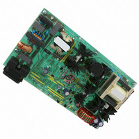
EVAL BOARD FOR NCP1605FORWG
Manufacturer
ON Semiconductor
Datasheets
1.NCP1217P100G.pdf
(19 pages)
2.NCP1605ADR2G.pdf
(32 pages)
3.NCP1605FORWGEVB.pdf
(2 pages)
4.NCP1605FORWGEVB.pdf
(20 pages)
Specifications of NCP1605FORWGEVB
Design Resources
NCP1605FORWGEVB BOM NCP1605FORWGEVB Gerber Files NCP1605 EVB Schematic
Main Purpose
AC/DC, Primary and Secondary Side with PFC
Outputs And Type
1, Isolated
Voltage - Output
19V
Current - Output
8A
Voltage - Input
90 ~ 265VAC
Regulator Topology
Forward Converter
Frequency - Switching
133kHz
Board Type
Fully Populated
Utilized Ic / Part
NCP1217, NCP1605
Lead Free Status / RoHS Status
Lead free / RoHS Compliant
Power - Output
-
Lead Free Status / Rohs Status
Lead free / RoHS Compliant
For Use With/related Products
NCP1605FORWG
Other names
NCP1605FORWGEVBOS


Brown−Out Detection
(V
integrate the ac line ripple so that a voltage proportional to
the average value of (V
conditions. A hysteresis comparator monitors the Pin 2
voltage. Before operation, the PFC stage is off and the input
bridge acts as a peak detector. Hence, the voltage applied
to Pin 2 is:
voltage becomes a rectified sinusoid and the voltage
applied to Pin 2 is:
Thermal Shutdown (TSD)
drive and then keeps the power switch off when the junction
temperature exceeds 150_C typically. The output stage is
then enabled once the temperature drops below about
100_C (50_C hysteresis).
circuit is not reset, that is, as long as V
V
be the upper one (150°C). This ensures that any cold startup
will be done with the right TSD level.
Output Drive Section
minimize the cross conduction current during high
frequency operation. The gate drive is kept in a sinking
mode whenever the Undervoltage Lockout is active or
more generally whenever the circuit is off (i.e., when the
“Fault Latch” of the block diagram is high or when the HV
current source is on). Its high current capability
(−500 mA/+800 mA) allows it to effectively drive high
gate charge power MOSFET.
Reference Section
voltage (V
the temperature range (the typical value is 2.5 V). V
Ac line
Filter
CC
EMI
The brown−out pin receives a portion of the input voltage
The brown−out block detects too low input voltage
After the PFC stage has started operation, the input
An internal thermal circuitry disables the circuit gate
The temperature shutdown keeps active as long as the
The output stage contains a totem pole optimized to
The circuit features an accurate internal reference
IN
RESET. The reset action forces the TSD threshold to
). As V
R
CS
REF
Figure 68. Brown−Out Block
IN
V pin2 + 2 Vac
). V
is a rectified sinusoid, a capacitor must
C
C
in
REF
bo2
Vin
is optimized to be ±3% accurate over
R
R
IN
bo1
bo2
BO
) is applied to the brown−out pin.
R bo1 ) R bo2
1 V / 0.5 V
R bo2
CC
+
-
keeps higher than
.
BO_NOK
http://onsemi.com
REF
is
400
200
27
0
i.e., about 64% of the previous value. Therefore, the same
line magnitude leads to a V
when the PFC is working than when it is off (refer to
Figure 69). That is why the NCP1605(A) features a 50%
hysteresis (V
equates the ac line peak.
Hence, the initial threshold of the Brown−Out
comparator, must be the upper one (V
when the NCP1605 leaves the off mode).
“BO_NOK” turns off the circuit (refer to block diagram).
the voltage reference used for the regulation and the
overvoltage protection. The circuit also incorporates a
precise current reference (I
Limitation to feature a ±6% accuracy over the temperature
range.
OFF Mode
following cases:
•
•
•
•
•
•
•
conditions are not proper for good operation. In this mode,
the controller stops operating. The major part of the circuit
sleeps and its consumption is minimized (< 500 mA).
When the circuit starts operation, the input voltage
When a brown−out condition is detected, the signal
As previously mentioned, the circuit turns off in the
Generally speaking, the circuit turns off when the
When the high voltage, startup current source charges
the V
When one of the following major faults is detected:
Incorrect feeding of the circuit (“UVLO” high when
V
Excessive die temperature detected by the thermal
shutdown.
Brown−Out condition.
Undervoltage Protection.
V
diagram turns high).
Figure 69. Typical Input Voltage of a PFC Stage
CC
Pin13
Start of PFC
Operation
<V
CC
2 @ Vac
higher than 2.5 V (“STDWN” of the block
CC
capacitor.
OFF, V
V pin2 +
BO
L = 50% V
CC
2 2 Vac
OFF equating 9 V typically).
p
REF
BO
Pin2
V
H).
) that allows the Overcurrent
SIN
R bo1 ) R bo2
voltage that is 36% lower
R bo2
2 @ Vac @ sin(Rt)
BO
= V
,
BO
H = 1 V
Related parts for NCP1605FORWGEVB
Image
Part Number
Description
Manufacturer
Datasheet
Request
R

Part Number:
Description:
ON Semiconductor [VOLTAGE REGULATOR]
Manufacturer:
ON Semiconductor
Datasheet:
Part Number:
Description:
357-036-542-201 CARDEDGE 36POS DL .156 BLK LOPRO
Manufacturer:
ON Semiconductor
Datasheet:
Part Number:
Description:
357-036-542-201 CARDEDGE 36POS DL .156 BLK LOPRO
Manufacturer:
ON Semiconductor
Datasheet:
Part Number:
Description:
357-036-542-201 CARDEDGE 36POS DL .156 BLK LOPRO
Manufacturer:
ON Semiconductor
Datasheet:
Part Number:
Description:
357-036-542-201 CARDEDGE 36POS DL .156 BLK LOPRO
Manufacturer:
ON Semiconductor
Datasheet:
Part Number:
Description:
357-036-542-201 CARDEDGE 36POS DL .156 BLK LOPRO
Manufacturer:
ON Semiconductor
Datasheet:
Part Number:
Description:
357-036-542-201 CARDEDGE 36POS DL .156 BLK LOPRO
Manufacturer:
ON Semiconductor
Datasheet:
Part Number:
Description:
357-036-542-201 CARDEDGE 36POS DL .156 BLK LOPRO
Manufacturer:
ON Semiconductor
Datasheet:
Part Number:
Description:
357-036-542-201 CARDEDGE 36POS DL .156 BLK LOPRO
Manufacturer:
ON Semiconductor
Datasheet:
Part Number:
Description:
357-036-542-201 CARDEDGE 36POS DL .156 BLK LOPRO
Manufacturer:
ON Semiconductor
Datasheet:
Part Number:
Description:
357-036-542-201 CARDEDGE 36POS DL .156 BLK LOPRO
Manufacturer:
ON Semiconductor
Datasheet:
Part Number:
Description:
Manufacturer:
ON Semiconductor
Datasheet:
Part Number:
Description:
Manufacturer:
ON Semiconductor
Datasheet:
Part Number:
Description:
Manufacturer:
ON Semiconductor
Datasheet: