NCP1605FORWGEVB ON Semiconductor, NCP1605FORWGEVB Datasheet - Page 19
NCP1605FORWGEVB
Manufacturer Part Number
NCP1605FORWGEVB
Description
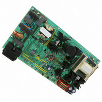
EVAL BOARD FOR NCP1605FORWG
Manufacturer
ON Semiconductor
Datasheets
1.NCP1217P100G.pdf
(19 pages)
2.NCP1605ADR2G.pdf
(32 pages)
3.NCP1605FORWGEVB.pdf
(2 pages)
4.NCP1605FORWGEVB.pdf
(20 pages)
Specifications of NCP1605FORWGEVB
Design Resources
NCP1605FORWGEVB BOM NCP1605FORWGEVB Gerber Files NCP1605 EVB Schematic
Main Purpose
AC/DC, Primary and Secondary Side with PFC
Outputs And Type
1, Isolated
Voltage - Output
19V
Current - Output
8A
Voltage - Input
90 ~ 265VAC
Regulator Topology
Forward Converter
Frequency - Switching
133kHz
Board Type
Fully Populated
Utilized Ic / Part
NCP1217, NCP1605
Lead Free Status / RoHS Status
Lead free / RoHS Compliant
Power - Output
-
Lead Free Status / Rohs Status
Lead free / RoHS Compliant
For Use With/related Products
NCP1605FORWG
Other names
NCP1605FORWGEVBOS


portrayed by Figure 55, the MOSFET on time t
controlled by the signal V
block and the Pin 4 ramp as follows:
[I
voltage (V
that is the capacitor connected between Pin 7 and ground
is also a constant. Hence, the power factor correction is
achieved when the
linearly changed into a signal (V
0 and 1 V. (V
PWM section to modulate the MOSFET duty−cycle.
However, like the NCP1601, the NCP1605(A) inserts some
circuitry that processes (V
(V
(V
to the dead−time sensed during the precedent current
cycles, that is, for a proper shaping of the ac line current
(refer to NCP1601 data sheet). This modulation leads to:
V TON +
pin7
Closed When
Output Low
The NCP1605(A) operates in voltage mode. As
The charge current that is sourced by Pin 7
The output of the regulation block (V
TON
REGUL
Figure 55. PWM Circuit and Timing Diagram
V
= 60 mA/V
) that is used in the PWM section instead of
in
) (see Figure 56). (V
Pin4
T @ V REGUL
Figure 53. PFC Boost Converter
REGUL
t 1 ) t 2
is proportional to the output voltage). C
2
I
in
* (V
t 1 +
V
) is the voltage that is injected into the
TON
C
ramp
I
Pin4
ch
C pin7 @ V TON
or : V TON @
(t
L
1
ton
)
PWM Comparator
V
2
+ t
ton
TON
] is constant at a given input
REGUL
I pin7
generated by the regulation
2
)/T
) is modulated in response
REGUL
Turns Off MOSFET
term is constant.
) to form the signal
V
Ramp Voltage
PWM Outtage
ton
t 1 ) t 2
) varying between
T
CONTROL
+ V REGUL
http://onsemi.com
(eq. 2)
(eq. 3)
V
1
) is
pin7
out
is
−> Vton during (t1+t2)
−> 0 V during t3 (dead−time)
−> Vton*(t1+t2)/T in average
19
V
REGUL
The integrator OA1 amplifies the error between V
(V
Hence, the (V
constant. Provided that in addition, (t1) is proportional to
(V
constant. More exactly:
voltage. Hence, the ac line current is properly shaped.
case. This condition is just a particular case of this
functioning where (t
(V
adapts to the conditions and jumps from DCM and CRM
(and vice versa) without power factor degradation and
without discontinuity in the power delivery.
circuit” is “informed” when there is an OVP condition, not
to over−dimension V
OVP sequence would be viewed as a dead−time phase by
the circuit and V
compensate it.
a skip sequence not to over−dimension “V
(refer to Figure 56).
IN1 so that in average, (V
I in + k @ V in
where : k + constant +
IN1
Given the regulation low bandwidth of the PFC systems,
The input current is then proportional to the input
One can note that this analysis is also valid in the CRM
Remark: Like in the NCP1601, the “V
Similarly, the “V
CONTROL
TON
TON
), equation (1) leads to: (I
= V
Figure 56. V
R1
REGUL
) and then (V
Figure 54. Inductor Current in DCM
+
TON
−
Inductor Current
). That is why the NCP1605 automatically
OA1
TON
timing capacitor
saw−tooth
TON
TON
C1
3
* (t
TON
t
1
= 0), which leads to (t
TON
S1
S2
would inappropriately increase to
V
Processing Circuit
processing circuit” is inhibited for
1
ton
REGUL
in that conditions. Otherwise, an
*(t1+t2)/T) equates V
+ t
120 m @ L @ (V pin2 )
C pin7 @ V REGUL
t
T
2
2
)/T) term is substantially
) are slow varying signals.
in
S3
= k * V
PWM
comparator
t
3
I
+
pk
−
(high during
dead−time)
REGUL
TON
in
TON
1
), where k is a
REGUL
to PWM latch
DT
+ t
2
” in this case
Time
processing
and
2
.
= T) and
(eq. 4)
SKIP
OFF
OVP
Related parts for NCP1605FORWGEVB
Image
Part Number
Description
Manufacturer
Datasheet
Request
R

Part Number:
Description:
ON Semiconductor [VOLTAGE REGULATOR]
Manufacturer:
ON Semiconductor
Datasheet:
Part Number:
Description:
357-036-542-201 CARDEDGE 36POS DL .156 BLK LOPRO
Manufacturer:
ON Semiconductor
Datasheet:
Part Number:
Description:
357-036-542-201 CARDEDGE 36POS DL .156 BLK LOPRO
Manufacturer:
ON Semiconductor
Datasheet:
Part Number:
Description:
357-036-542-201 CARDEDGE 36POS DL .156 BLK LOPRO
Manufacturer:
ON Semiconductor
Datasheet:
Part Number:
Description:
357-036-542-201 CARDEDGE 36POS DL .156 BLK LOPRO
Manufacturer:
ON Semiconductor
Datasheet:
Part Number:
Description:
357-036-542-201 CARDEDGE 36POS DL .156 BLK LOPRO
Manufacturer:
ON Semiconductor
Datasheet:
Part Number:
Description:
357-036-542-201 CARDEDGE 36POS DL .156 BLK LOPRO
Manufacturer:
ON Semiconductor
Datasheet:
Part Number:
Description:
357-036-542-201 CARDEDGE 36POS DL .156 BLK LOPRO
Manufacturer:
ON Semiconductor
Datasheet:
Part Number:
Description:
357-036-542-201 CARDEDGE 36POS DL .156 BLK LOPRO
Manufacturer:
ON Semiconductor
Datasheet:
Part Number:
Description:
357-036-542-201 CARDEDGE 36POS DL .156 BLK LOPRO
Manufacturer:
ON Semiconductor
Datasheet:
Part Number:
Description:
357-036-542-201 CARDEDGE 36POS DL .156 BLK LOPRO
Manufacturer:
ON Semiconductor
Datasheet:
Part Number:
Description:
Manufacturer:
ON Semiconductor
Datasheet:
Part Number:
Description:
Manufacturer:
ON Semiconductor
Datasheet:
Part Number:
Description:
Manufacturer:
ON Semiconductor
Datasheet: