EVAL-ADUC812QS Analog Devices Inc, EVAL-ADUC812QS Datasheet - Page 25
EVAL-ADUC812QS
Manufacturer Part Number
EVAL-ADUC812QS
Description
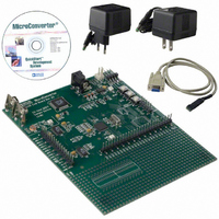
KIT DEV FOR ADUC812 QUICK START
Manufacturer
Analog Devices Inc
Series
QuickStart™ Kitr
Type
MCUr
Datasheet
1.EVAL-ADUC812QS.pdf
(60 pages)
Specifications of EVAL-ADUC812QS
Rohs Status
RoHS non-compliant
Contents
Evaluation Board, Power Supply, Cable, Software and Documentation
For Use With/related Products
ADuC812


PSMCON
SFR Address
Power-On Default Value
Bit Addressable
Bit
7
6
5
4
3
2
1
0
Example
To configure the PSM for a trip point of 4.37 V, the following
code would be used:
MOV
SETB
MOV
If the supply voltage falls below this level, the PC would vector
to the ISR.
ORG
CHECK:MOV
JB
RETI
REV. E
—
PSMCON,#005h
EA
IE2,#002h
Name
—
CMP
PSMI
TP2
TP1
TP0
PSF
PSMEN
0043h
A,PSMCON
ACC.5,CHECK
; return only when "all's well"
C
M
P
;enable PSM with
Power Supply Monitor
Control Register
DFH
DCH
No
Description
Not Used.
AV
This is a read-only bit and directly reflects the state of the AV
Read “1” indicates that both the AV
Read “0” indicates that either the AV
Power Supply Monitor Interrupt Bit.
This bit will be set high by the MicroConverter if CMP is low, indicating low analog or digital
supply. The PSMI bit can be used to interrupt the processor. Once CMPD and/or CMP return
(and remain) high, a 256 ms counter is started. When this counter times out, the PSMI interrupt
is cleared. PSMI can also be written by the user. However, if either comparator output is low,
it is not possible for the user to clear PSMI.
V
These bits select the AV
TP2
0
0
0
0
1
AV
Read “1” indicates that the AV
Read “0” indicates that the DV
Power Supply Monitor Enable Bit.
Set to “1” by the user to enable the Power Supply Monitor Circuit.
Cleared to “0” by the user to disable the Power Supply Monitor Circuit.
;4.37V threshold
;enable interrupts
;enable PSM
;interrupt
DD
P
DD
DD
S
;PSM ISR
;PSMCON.5 is the
;PSM interrupt
;bit..
;..it is cleared
;only when Vdd
;has remained
;above the trip
;point for 256ms
;or more.
M
Trip Point Selection Bits.
/DV
and DV
I
Table X. PSMCON SFR Bit Designations
DD
TP1
0
0
1
1
0
Fault Indicator.
DD
Comparator Bit.
T
P
2
DD
TP0
0
1
0
1
0
and DV
–25–
DD
DD
SERIAL PERIPHERAL INTERFACE
The ADuC812 integrates a complete hardware Serial Peripheral
Interface (SPI) on-chip. SPI is an industry-standard synchronous
serial interface that allows eight bits of data to be synchronously
transmitted and received simultaneously, i.e., full duplex. It should
be noted that the SPI pins are shared with the I
therefore the user can only enable one or the other interface at
any given time (see SPE in Table XI). The SPI Port can be con-
figured for Master or Slave operation and typically consists of
four pins, namely:
MISO (Master In, Slave Out Data I/O Pin)
The MISO (master in, slave out) pin is configured as an input
line in master mode and an output line in slave mode. The
MISO line on the master (data in) should be connected to the
MISO line in the slave device (data out). The data is transferred
as byte wide (8-bit) serial data, MSB first.
supply caused the fault condition.
supply caused the fault condition.
DD
Selected DV
4.63
4.37
3.08
2.93
2.63
T
DD
DD
P
trip point voltage as follows:
1
and DV
or DV
DD
DD
DD
supply is below its selected trip point.
supplies are above their selected trip points.
Trip Point (V)
T
P
0
DD
and DV
P
S
F
DD
comparators.
ADuC812
2
C interface, and
P
S
M
E
N
Related parts for EVAL-ADUC812QS
Image
Part Number
Description
Manufacturer
Datasheet
Request
R


Part Number:
Description:
BOARD EVAL FOR SI270X-A
Manufacturer:
Silicon Laboratories Inc
Datasheet:

Part Number:
Description:
BUCK CONV REF DESIGN KIT IP1201
Manufacturer:
International Rectifier
Datasheet:
Part Number:
Description:
BOARD DEMO SYNC DUAL BUCK CNVTER
Manufacturer:
International Rectifier
Datasheet:
Part Number:
Description:
BOARD DEMO SYNC BUCK CONVETER
Manufacturer:
International Rectifier
Datasheet:

Part Number:
Description:
EVALBOARD/EB Omnidirectional microphone - Analog
Manufacturer:
Analog Devices
Datasheet:
Part Number:
Description:
EVALBOARD/EB Omnidirectional microphone - Analog
Manufacturer:
Analog Devices
Datasheet:


Part Number:
Description:
BOARD EVAL LED DRIVER LT3756
Manufacturer:
Linear Technology
Datasheet:

Part Number:
Description:
BOARD EVAL FOR AD7741/7742
Manufacturer:
Analog Devices Inc
Datasheet:

Part Number:
Description:
±1.7g Dual-Axis IMEMS Accelerometer Evaluation Board
Manufacturer:
Analog Devices Inc
Datasheet:

Part Number:
Description:
IC MULTIPLIER ANALOG 8-SOIC T/R
Manufacturer:
Analog Devices Inc
Datasheet:

Part Number:
Description:
IC ANALOG MULTIPLIER 8-DIP
Manufacturer:
Analog Devices Inc
Datasheet:
Part Number:
Description:
IC ANALOG MULTIPLIER 8-SOIC
Manufacturer:
Analog Devices Inc
Datasheet:
Part Number:
Description:
IC ANALOG MULTIPLIER 8-DIP
Manufacturer:
Analog Devices Inc
Datasheet: