EVAL-ADUC812QS Analog Devices Inc, EVAL-ADUC812QS Datasheet - Page 46
EVAL-ADUC812QS
Manufacturer Part Number
EVAL-ADUC812QS
Description
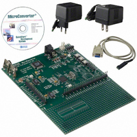
KIT DEV FOR ADUC812 QUICK START
Manufacturer
Analog Devices Inc
Series
QuickStart™ Kitr
Type
MCUr
Datasheet
1.EVAL-ADUC812QS.pdf
(60 pages)
Specifications of EVAL-ADUC812QS
Rohs Status
RoHS non-compliant
Contents
Evaluation Board, Power Supply, Cable, Software and Documentation
For Use With/related Products
ADuC812


TIMING SPECIFICATIONS
ADuC812
Parameter
CLOCK INPUT (External Clock Driven XTAL1)
t
t
t
t
t
t
NOTES
1
2
3
4
AC inputs during testing are driven at DV
For timing purposes, a port pin is no longer floating when a 100 mV change from load voltage occurs. A port pin begins to float when a 100 mV change from the
C
ADuC812 Machine Cycle Time is nominally defined as MCLKIN/12.
CK
CKL
CKH
CKR
CKF
CYC
a Logic 0.
loaded V
LOAD
4
for Port 0, ALE, PSEN outputs = 100 pF; C
OH
/V
OL
level occurs.
DV
XTAL1 Period
XTAL1 Width Low
XTAL1 Width High
XTAL1 Rise Time
XTAL1 Fall Time
ADuC812 Machine Cycle Time
DD
– 0.5V
0.45V
DD
– 0.5 V for a Logic 1 and 0.45 V for a Logic 0. Timing measurements are made at V
1, 2, 3
0.2V
TEST POINTS
0.2V
LOAD
CC
CC
Figure 50. Timing Waveform Characteristics
+ 0.9V
– 0.1V
(AV
for all other outputs = 80 pF, unless otherwise noted.
t
DD
CKH
= DV
Figure 49. XTAL 1 Input
DD
= 3.0 V or 5.0 V
Min
20
20
V
–46–
LOAD
t
CKL
12 MHz
Typ
83.33
1
V
V
LOAD
LOAD
– 0.1V
+ 0.1V
10%. All specifications T
t
CKR
Max
20
20
t
CK
REFERENCE
POINTS
TIMING
Min
62.5
20
20
Variable Clock
t
CKF
Typ
12t
A
= T
CK
MIN
V
V
LOAD
LOAD
IH
to T
min for a Logic 1 and V
Max
1000
20
20
– 0.1V
– 0.1V
MAX
, unless otherwise noted.)
V
LOAD
Unit
ns
µs
ns
ns
ns
ns
IL
REV. E
max for
Related parts for EVAL-ADUC812QS
Image
Part Number
Description
Manufacturer
Datasheet
Request
R


Part Number:
Description:
BOARD EVAL FOR SI270X-A
Manufacturer:
Silicon Laboratories Inc
Datasheet:

Part Number:
Description:
BUCK CONV REF DESIGN KIT IP1201
Manufacturer:
International Rectifier
Datasheet:
Part Number:
Description:
BOARD DEMO SYNC DUAL BUCK CNVTER
Manufacturer:
International Rectifier
Datasheet:
Part Number:
Description:
BOARD DEMO SYNC BUCK CONVETER
Manufacturer:
International Rectifier
Datasheet:

Part Number:
Description:
EVALBOARD/EB Omnidirectional microphone - Analog
Manufacturer:
Analog Devices
Datasheet:
Part Number:
Description:
EVALBOARD/EB Omnidirectional microphone - Analog
Manufacturer:
Analog Devices
Datasheet:


Part Number:
Description:
BOARD EVAL LED DRIVER LT3756
Manufacturer:
Linear Technology
Datasheet:

Part Number:
Description:
BOARD EVAL FOR AD7741/7742
Manufacturer:
Analog Devices Inc
Datasheet:

Part Number:
Description:
±1.7g Dual-Axis IMEMS Accelerometer Evaluation Board
Manufacturer:
Analog Devices Inc
Datasheet:

Part Number:
Description:
IC MULTIPLIER ANALOG 8-SOIC T/R
Manufacturer:
Analog Devices Inc
Datasheet:

Part Number:
Description:
IC ANALOG MULTIPLIER 8-DIP
Manufacturer:
Analog Devices Inc
Datasheet:
Part Number:
Description:
IC ANALOG MULTIPLIER 8-SOIC
Manufacturer:
Analog Devices Inc
Datasheet:
Part Number:
Description:
IC ANALOG MULTIPLIER 8-DIP
Manufacturer:
Analog Devices Inc
Datasheet: