EVAL-ADUC812QS Analog Devices Inc, EVAL-ADUC812QS Datasheet - Page 26
EVAL-ADUC812QS
Manufacturer Part Number
EVAL-ADUC812QS
Description
KIT DEV FOR ADUC812 QUICK START
Manufacturer
Analog Devices Inc
Series
QuickStart™ Kitr
Type
MCUr
Datasheet
1.EVAL-ADUC812QS.pdf
(60 pages)
Specifications of EVAL-ADUC812QS
Rohs Status
RoHS non-compliant
Contents
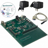
Evaluation Board, Power Supply, Cable, Software and Documentation
For Use With/related Products
ADuC812


ADuC812
MOSI (Master Out, Slave In Pin)
The MOSI (master out, slave in) pin is configured as an output
line in master mode and an input line in slave mode. The
MOSI line on the master (data out) should be connected to the
MOSI line in the slave device (data in). The data is transferred as
byte wide (8-bit) serial data, MSB first.
SCLOCK (Serial Clock I/O Pin)
The master serial clock (SCLOCK) is used to synchronize the
data being transmitted and received through the MOSI and MISO
data lines. A single data bit is transmitted and received in each
SCLOCK period. Therefore, a byte is transmitted/received after
eight SCLOCK periods. The SCLOCK pin is configured as an
output in master mode and as an input in slave mode. In master
mode, the bit rate, polarity, and phase of the clock are controlled
by the CPOL, CPHA, SPR0, and SPR1 bits in the SPICON SFR
(see Table XI). In slave mode, the SPICON register will have to
be configured with the phase and polarity (CPHA and CPOL) of
the expected input clock. In both master and slave modes, the
SPICON
SFR Address
Power-On Default Value
Bit Addressable
Bit
7
6
5
4
3
2
1
0
*The CPOL and CPHA bits should both contain the same values for master and slave devices.
I
S
P
I
Name
ISPI
WCOL
SPE
SPIM
CPOL*
CPHA*
SPR1
SPR0
W
C
O
L
SPI Control
Register
F8H
OOH
Yes
SPI Interrupt Bit.
Write Collision Error Bit.
SPI Interface Enable Bit.
SPI Master/Slave Mode Select Bit.
SPI Bit Rate Select Bits.
These bits select the SCLOCK rate (bit rate) in Master mode as follows:
Description
Set by MicroConverter at the end of each SPI transfer.
Cleared directly by user code or indirectly by reading the SPIDAT SFR.
Set by MicroConverter if SPIDAT is written to while an SPI transfer is in progress.
Cleared by user code.
Set by user to enable the SPI interface.
Cleared by user to enable I
Set by user to enable Master mode operation (SCLOCK is an output).
Cleared by user to enable Slave mode operation (SCLOCK is an input).
Clock Polarity Select Bit.
Set by user if SCLOCK idles high.
Cleared by user if SCLOCK idles low.
Clock Phase Select Bit.
Set by user if leading SCLOCK edge is to transmit data.
Cleared by user if trailing SCLOCK edge is to transmit data.
SPR1
0
0
1
1
In SPI Slave mode, i.e., SPIM = 0, the logic level on the external SS pin can be read
via the SPR0 bit.
S
P
E
Table XI. SPICON SFR Bit Designations
SPR0
0
1
0
1
S
P
I
M
Selected Bit Rate
f
f
f
f
OSC
OSC
OSC
OSC
/4
/8
/32
/64
2
–26–
C interface.
data is transmitted on one edge of the SCLOCK signal and
sampled on the other. It is important therefore that the CPHA
and CPOL are configured the same for the master and slave
devices.
SS (Slave Select Input Pin)
The Slave Select (SS) input pin is shared with the ADC5 input.
To configure this pin as a digital input, the bit must be cleared,
e.g., CLR P1.5.
This line is active low. Data is only received or transmitted in
slave mode when the SS pin is low, allowing the ADuC812 to
be used in single master, multislave SPI configurations. If
CPHA = 1, then the SS input may be permanently pulled low.
With CPHA = 0, the SS input must be driven low before the
first bit in a byte wide transmission or reception, and return
high again after the last bit in that byte wide transmission or
reception. In SPI Slave mode, the logic level on the external SS
pin can be read via the SPR0 bit in the SPICON SFR. The follow-
ing SFR registers are used to control the SPI interface.
C
P
O
L
C
P
H
A
S
P
R
1
S
P
R
0
REV. E
Related parts for EVAL-ADUC812QS
Image
Part Number
Description
Manufacturer
Datasheet
Request
R


Part Number:
Description:
BOARD EVAL FOR SI270X-A
Manufacturer:
Silicon Laboratories Inc
Datasheet:

Part Number:
Description:
BUCK CONV REF DESIGN KIT IP1201
Manufacturer:
International Rectifier
Datasheet:
Part Number:
Description:
BOARD DEMO SYNC DUAL BUCK CNVTER
Manufacturer:
International Rectifier
Datasheet:
Part Number:
Description:
BOARD DEMO SYNC BUCK CONVETER
Manufacturer:
International Rectifier
Datasheet:

Part Number:
Description:
EVALBOARD/EB Omnidirectional microphone - Analog
Manufacturer:
Analog Devices
Datasheet:
Part Number:
Description:
EVALBOARD/EB Omnidirectional microphone - Analog
Manufacturer:
Analog Devices
Datasheet:


Part Number:
Description:
BOARD EVAL LED DRIVER LT3756
Manufacturer:
Linear Technology
Datasheet:

Part Number:
Description:
BOARD EVAL FOR AD7741/7742
Manufacturer:
Analog Devices Inc
Datasheet:

Part Number:
Description:
±1.7g Dual-Axis IMEMS Accelerometer Evaluation Board
Manufacturer:
Analog Devices Inc
Datasheet:

Part Number:
Description:
IC MULTIPLIER ANALOG 8-SOIC T/R
Manufacturer:
Analog Devices Inc
Datasheet:

Part Number:
Description:
IC ANALOG MULTIPLIER 8-DIP
Manufacturer:
Analog Devices Inc
Datasheet:
Part Number:
Description:
IC ANALOG MULTIPLIER 8-SOIC
Manufacturer:
Analog Devices Inc
Datasheet:
Part Number:
Description:
IC ANALOG MULTIPLIER 8-DIP
Manufacturer:
Analog Devices Inc
Datasheet: