EVAL-ADUC812QS Analog Devices Inc, EVAL-ADUC812QS Datasheet - Page 40
EVAL-ADUC812QS
Manufacturer Part Number
EVAL-ADUC812QS
Description
KIT DEV FOR ADUC812 QUICK START
Manufacturer
Analog Devices Inc
Series
QuickStart™ Kitr
Type
MCUr
Datasheet
1.EVAL-ADUC812QS.pdf
(60 pages)
Specifications of EVAL-ADUC812QS
Rohs Status
RoHS non-compliant
Contents
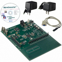
Evaluation Board, Power Supply, Cable, Software and Documentation
For Use With/related Products
ADuC812


ADuC812
ADuC812 HARDWARE DESIGN CONSIDERATIONS
This section outlines some of the key hardware design consider-
ations that must be addressed when integrating the ADuC812
into any hardware system.
Clock Oscillator
The clock source for the ADuC812 can come either from an
external source or from the internal clock oscillator. To use the
internal clock oscillator, connect a parallel resonant crystal
between Pins 32 and 33, and connect a capacitor from each pin
to ground as shown below.
Whether using the internal oscillator or an external clock source,
the ADuC812’s specified operational clock speed range is 300 kHz
to 16 MHz. The core is static, and will function all the way
down to dc. But at clock speeds slower that 400 kHz the ADC
will no longer function correctly. Therefore, to ensure specified
operation, use a clock frequency of at least 400 kHz and no
more than 16 MHz.
External Memory Interface
In addition to its internal program and data memories, the
ADuC812 can access up to 64 K bytes of external program
memory (ROM, PROM, etc.) and up to 16 M bytes of exter-
nal data memory (SRAM).
To select from which code space (internal or external program
memory) to begin executing instructions, tie the EA (external
access) pin high or low, respectively. When EA is high (pulled
up to V
internal 8 K bytes Flash/EE code space. When EA is low (tied
to ground) user program execution will start at address 0 of the
external code space. In either case, addresses above 1FFFH
(8K) are mapped to the external space.
Note that a second very important function of the EA pin is
described in the Single Pin Emulation Mode section.
Figure 35. External Parallel Resonant Crystal Connections
Figure 36. Connecting an External Clock Source
DD
EXTERNAL
SOURCE
), user program execution will start at address 0 of the
CLOCK
XTAL1
XTAL2
XTAL1
XTAL2
ADuC812
ADuC812
TO INTERNAL
TIMING CIRCUITS
TO INTERNAL
TIMING CIRCUITS
–40–
External program memory (if used) must be connected to the
ADuC812 as illustrated in Figure 37. Note that 16 I/O lines
(Ports 0 and 2) are dedicated to bus functions during external
program memory fetches. Port 0 (P0) serves as a multiplexed
address/data bus. It emits the low byte of the program counter
(PCL) as an address, and then goes into a float state awaiting
the arrival of the code byte from the program memory. During
the time that the low byte of the program counter is valid on P0,
the signal ALE (Address Latch Enable) clocks this byte into an
address latch. Meanwhile, Port 2 (P2) emits the high byte of the
program counter (PCH), then PSEN strobes the EPROM and
the code byte is read into the ADuC812.
Note that program memory addresses are always 16 bits wide, even
in cases where the actual amount of program memory used is less
than 64 K bytes. External program execution sacrifices two of the
8-bit ports (P0 and P2) to the function of addressing the program
memory. While executing from external program memory, Ports 0
and 2 can be used simultaneously for read/write access to external
data memory, but not for general-purpose I/O.
Though both external program memory and external data memory
are accessed by some of the same pins, the two are completely
independent of each other from a software point of view. For example,
the chip can read/write external data memory while executing
from external program memory.
Figure 38 shows a hardware configuration for accessing up to
64 K bytes of external RAM. This interface is standard to any
8051 compatible MCU.
Figure 37. External Program Memory Interface
Figure 38. External Data Memory Interface
(64K Address Space)
ADuC812
ADuC812
PSEN
ALE
ALE
P0
P2
WR
RD
P2
P0
LATCH
LATCH
OE
D0–D7
(INSTRUCTION)
A0–A7
A8–A15
OE
WE
D0–D7
(DATA)
A0–A7
A8–A15
EPROM
SRAM
REV. E
Related parts for EVAL-ADUC812QS
Image
Part Number
Description
Manufacturer
Datasheet
Request
R


Part Number:
Description:
BOARD EVAL FOR SI270X-A
Manufacturer:
Silicon Laboratories Inc
Datasheet:

Part Number:
Description:
BUCK CONV REF DESIGN KIT IP1201
Manufacturer:
International Rectifier
Datasheet:
Part Number:
Description:
BOARD DEMO SYNC DUAL BUCK CNVTER
Manufacturer:
International Rectifier
Datasheet:
Part Number:
Description:
BOARD DEMO SYNC BUCK CONVETER
Manufacturer:
International Rectifier
Datasheet:

Part Number:
Description:
EVALBOARD/EB Omnidirectional microphone - Analog
Manufacturer:
Analog Devices
Datasheet:
Part Number:
Description:
EVALBOARD/EB Omnidirectional microphone - Analog
Manufacturer:
Analog Devices
Datasheet:


Part Number:
Description:
BOARD EVAL LED DRIVER LT3756
Manufacturer:
Linear Technology
Datasheet:

Part Number:
Description:
BOARD EVAL FOR AD7741/7742
Manufacturer:
Analog Devices Inc
Datasheet:

Part Number:
Description:
±1.7g Dual-Axis IMEMS Accelerometer Evaluation Board
Manufacturer:
Analog Devices Inc
Datasheet:

Part Number:
Description:
IC MULTIPLIER ANALOG 8-SOIC T/R
Manufacturer:
Analog Devices Inc
Datasheet:

Part Number:
Description:
IC ANALOG MULTIPLIER 8-DIP
Manufacturer:
Analog Devices Inc
Datasheet:
Part Number:
Description:
IC ANALOG MULTIPLIER 8-SOIC
Manufacturer:
Analog Devices Inc
Datasheet:
Part Number:
Description:
IC ANALOG MULTIPLIER 8-DIP
Manufacturer:
Analog Devices Inc
Datasheet: