EVAL-ADUC812QS Analog Devices Inc, EVAL-ADUC812QS Datasheet - Page 28
EVAL-ADUC812QS
Manufacturer Part Number
EVAL-ADUC812QS
Description
KIT DEV FOR ADUC812 QUICK START
Manufacturer
Analog Devices Inc
Series
QuickStart™ Kitr
Type
MCUr
Datasheet
1.EVAL-ADUC812QS.pdf
(60 pages)
Specifications of EVAL-ADUC812QS
Rohs Status
RoHS non-compliant
Contents
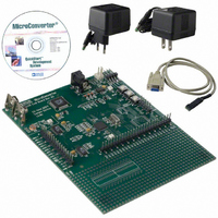
Evaluation Board, Power Supply, Cable, Software and Documentation
For Use With/related Products
ADuC812


ADuC812
I
The ADuC812 supports a 2-wire serial interface mode that is
I
the on-chip SPI interface and therefore the user can only enable
one or the other interface at any given time (see SPE in Table IX).
An application note describing the operation of this interface as
implemented is available from the MicroConverter website at
www.analog.com/microconverter. This interface can be configured
as a software master or hardware slave, and uses two pins in the
interface.
Bit
7
6
5
4
3
2
1
0
I2CADD
Function
SFR Address
Power-On Default Value 55H
Bit Addressable
*Purchase of licensed I
I
2
2
2
C* COMPATIBLE INTERFACE
C compatible. The I
C Patent Rights to use these components in an I
M
D
O
Name
MDO
MDE
MCO
MDI
I2CM
I2CRS
I2CTX
I2CI
2
C components of Analog Devices or one of its sublicensed Associated Companies conveys a license for the purchaser under the Philips
2
M
C compatible interface shares its pins with
D
I
Holds the I
the part. It may be overwritten by
the user code. Application note uC001
at www.analog.com/microconverter
describes the format of the I
standard 7-bit address in detail.
9BH
No
E
2
C Address Register
Description
I
This data bit is used to implement a master I
this bit will be output on the SDATA pin if the data output enable (MDE) bit is set.
I
Set by the user to enable the SDATA pin as an output (Tx). Cleared by the user to enable SDATA
pin as an input (Rx).
I
This data bit is used to implement a master I
this bit will be output on the SCLOCK pin.
I
This data bit is used to implement a master I
SDATA pin is latched into this bit on SCLOCK if the Data Output Enable (MDE) = 0.
I
Set by user to enable I
I
Set by user to reset the I
I
Set by the MicroConverter if the interface is transmitting. Cleared by the MicroConverter if the
interface is receiving.
I
Set by the MicroConverter after a byte has been transmitted or received. Cleared by user software.
2
2
2
2
2
2
2
2
C Software Master Data Output Bit (Master Mode Only).
C Software Master Data Output Enable Bit (Master Mode Only).
C Software Master Data Output Bit (Master Mode Only).
C Software Master Data Input Bit (Master Mode Only).
C Master/Slave Mode Bit.
C Reset Bit (Slave Mode Only).
C Direction Transfer Bit (Slave Mode Only).
C Interrupt Bit (Slave Mode Only).
2
M
C peripheral address for
C
O
2
C system, provided that the system conforms to the I
Table XII. I2CCON SFR Bit Designations
2
C
2
M
C software master mode. Cleared by user to enable I
D
2
C interface. Cleared by user for normal I
I
–28–
SDATA
SCLOCK
Three SFRs are used to control the I
These are described below:
I2CCON
SFR Address
Power-On Default Value
Bit Addressable
I2CDAT
Function
SFR Address
Power-On Default Value 00H
Bit Addressable
2 I
C
M
2
2
2
C transmitter interface in software. Data written to
C transmitter interface in software. Data written to
C receiver interface in software. Data on the
2 I
2
C Standard Specification as defined by Philips.
C
R
S
The I2CDAT SFR is written by the
I
user to transmit data over the I
interface or read by user code to read
data just received by the I
User software should only access
I2CDAT once per interrupt cycle.
9AH
No
2
C Data Register
2
C operation.
2 I
Serial Data I/O Pin
Serial Clock
I
2
E8H
00H
Yes
C
C compatible interface.
2
C Control Register
T
2
C hardware slave mode.
X
2
2 I
C interface.
C
I
REV. E
2
C
Related parts for EVAL-ADUC812QS
Image
Part Number
Description
Manufacturer
Datasheet
Request
R


Part Number:
Description:
BOARD EVAL FOR SI270X-A
Manufacturer:
Silicon Laboratories Inc
Datasheet:

Part Number:
Description:
BUCK CONV REF DESIGN KIT IP1201
Manufacturer:
International Rectifier
Datasheet:
Part Number:
Description:
BOARD DEMO SYNC DUAL BUCK CNVTER
Manufacturer:
International Rectifier
Datasheet:
Part Number:
Description:
BOARD DEMO SYNC BUCK CONVETER
Manufacturer:
International Rectifier
Datasheet:

Part Number:
Description:
EVALBOARD/EB Omnidirectional microphone - Analog
Manufacturer:
Analog Devices
Datasheet:
Part Number:
Description:
EVALBOARD/EB Omnidirectional microphone - Analog
Manufacturer:
Analog Devices
Datasheet:


Part Number:
Description:
BOARD EVAL LED DRIVER LT3756
Manufacturer:
Linear Technology
Datasheet:

Part Number:
Description:
BOARD EVAL FOR AD7741/7742
Manufacturer:
Analog Devices Inc
Datasheet:

Part Number:
Description:
±1.7g Dual-Axis IMEMS Accelerometer Evaluation Board
Manufacturer:
Analog Devices Inc
Datasheet:

Part Number:
Description:
IC MULTIPLIER ANALOG 8-SOIC T/R
Manufacturer:
Analog Devices Inc
Datasheet:

Part Number:
Description:
IC ANALOG MULTIPLIER 8-DIP
Manufacturer:
Analog Devices Inc
Datasheet:
Part Number:
Description:
IC ANALOG MULTIPLIER 8-SOIC
Manufacturer:
Analog Devices Inc
Datasheet:
Part Number:
Description:
IC ANALOG MULTIPLIER 8-DIP
Manufacturer:
Analog Devices Inc
Datasheet: