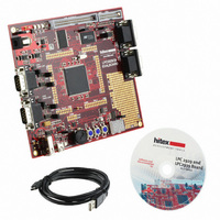
OM11027 NXP Semiconductors, OM11027 Datasheet - Page 20

OM11027
Manufacturer Part Number
OM11027
Description
BOARD EVAL LPC2939
Manufacturer
NXP Semiconductors
Type
MCUr
Datasheet
1.OM11027.pdf
(99 pages)
Specifications of OM11027
Contents
Board
For Use With/related Products
LPC2939
Lead Free Status / RoHS Status
Lead free / RoHS Compliant
Other names
568-4787
- Current page: 20 of 99
- Download datasheet (2Mb)
NXP Semiconductors
LPC2939_3
Product data sheet
6.7.2 Base clock and branch clock relationship
Table 7
branch clocks. A short description is given of the hardware parts that are clocked with the
individual branch clocks. In relevant cases more detailed information can be found in the
specific subsystem description. Some branch clocks have special protection since they
clock vital system parts of the device and should not be switched off. See
for more details of how to control the individual branch clocks.
Table 7.
Base clock
BASE_SAFE_CLK
BASE_SYS_CLK
BASE_PCR_CLK
BASE_IVNSS_CLK
contains an overview of all the base blocks in the LPC2939 and their derived
CGU0 base clock and branch clock overview
All information provided in this document is subject to legal disclaimers.
Branch clock name
CLK_SAFE
CLK_SYS_CPU
CLK_SYS_SYS
CLK_SYS_PCRSS
CLK_SYS_FMC
CLK_SYS_RAM0
CLK_SYS_RAM1
CLK_SYS_SMC
CLK_SYS_GESS
CLK_SYS_VIC
CLK_SYS_PESS
CLK_SYS_GPIO0
CLK_SYS_GPIO1
CLK_SYS_GPIO2
CLK_SYS_GPIO3
CLK_SYS_GPIO4
CLK_SYS_GPIO5
CLK_SYS_IVNSS_A
CLK_SYS_MSCSS_A
CLK_SYS_DMA
CLK_SYS_USB
CLK_PCR_SLOW
CLK_IVNSS_APB
CLK_IVNSS_CANCA
CLK_IVNSS_CANC0
CLK_IVNSS_CANC1
CLK_IVNSS_I2C0
CLK_IVNSS_I2C1
CLK_IVNSS_LIN0
CLK_IVNSS_LIN1
Rev. 03 — 7 April 2010
ARM9 microcontroller with CAN, LIN, and USB
Parts of the device clocked by this
branch clock
watchdog timer
ARM968E-S and TCMs
AHB bus infrastructure
AHB side of bridge in PCRSS
flash memory controller
embedded SRAM controller 0 (32 kB)
embedded SRAM controller 1 (16 kB)
external Static Memory Controller
(SMC)
General SubSystem (GESS)
Vectored Interrupt Controller (VIC)
Peripheral SubSystem (PESS)
GPIO bank 0
GPIO bank 1
GPIO bank 2
GPIO bank 3
GPIO bank 4
GPIO bank 5
AHB side of bridge of IVNSS
AHB side of bridge of MSCSS
GPDMA
USB registers
PCRSS, CGU, RGU and PMU logic
clock
APB side of the IVNSS
CAN controller Acceptance Filter
CAN channel 0
CAN channel 1
I
I
LIN channel 0
LIN channel 1
2
2
C0
C1
LPC2939
© NXP B.V. 2010. All rights reserved.
Section 6.16.5
20 of 99
[2] [4]
[1] [3]
[1]
Related parts for OM11027
Image
Part Number
Description
Manufacturer
Datasheet
Request
R
Part Number:
Description:
NXP Semiconductors designed the LPC2420/2460 microcontroller around a 16-bit/32-bitARM7TDMI-S CPU core with real-time debug interfaces that include both JTAG andembedded trace
Manufacturer:
NXP Semiconductors
Datasheet:

Part Number:
Description:
NXP Semiconductors designed the LPC2458 microcontroller around a 16-bit/32-bitARM7TDMI-S CPU core with real-time debug interfaces that include both JTAG andembedded trace
Manufacturer:
NXP Semiconductors
Datasheet:
Part Number:
Description:
NXP Semiconductors designed the LPC2468 microcontroller around a 16-bit/32-bitARM7TDMI-S CPU core with real-time debug interfaces that include both JTAG andembedded trace
Manufacturer:
NXP Semiconductors
Datasheet:
Part Number:
Description:
NXP Semiconductors designed the LPC2470 microcontroller, powered by theARM7TDMI-S core, to be a highly integrated microcontroller for a wide range ofapplications that require advanced communications and high quality graphic displays
Manufacturer:
NXP Semiconductors
Datasheet:
Part Number:
Description:
NXP Semiconductors designed the LPC2478 microcontroller, powered by theARM7TDMI-S core, to be a highly integrated microcontroller for a wide range ofapplications that require advanced communications and high quality graphic displays
Manufacturer:
NXP Semiconductors
Datasheet:
Part Number:
Description:
The Philips Semiconductors XA (eXtended Architecture) family of 16-bit single-chip microcontrollers is powerful enough to easily handle the requirements of high performance embedded applications, yet inexpensive enough to compete in the market for hi
Manufacturer:
NXP Semiconductors
Datasheet:
Part Number:
Description:
The XA-S3 device is a member of Philips Semiconductors? XA(eXtended Architecture) family of high performance 16-bitsingle-chip microcontrollers
Manufacturer:
NXP Semiconductors
Datasheet:

Part Number:
Description:
The NXP BlueStreak LH75401/LH75411 family consists of two low-cost 16/32-bit System-on-Chip (SoC) devices
Manufacturer:
NXP Semiconductors
Datasheet:

Part Number:
Description:
The NXP LPC3130/3131 combine an 180 MHz ARM926EJ-S CPU core, high-speed USB2
Manufacturer:
NXP Semiconductors
Datasheet:

Part Number:
Description:
The NXP LPC3141 combine a 270 MHz ARM926EJ-S CPU core, High-speed USB 2
Manufacturer:
NXP Semiconductors

Part Number:
Description:
The NXP LPC3143 combine a 270 MHz ARM926EJ-S CPU core, High-speed USB 2
Manufacturer:
NXP Semiconductors

Part Number:
Description:
The NXP LPC3152 combines an 180 MHz ARM926EJ-S CPU core, High-speed USB 2
Manufacturer:
NXP Semiconductors

Part Number:
Description:
The NXP LPC3154 combines an 180 MHz ARM926EJ-S CPU core, High-speed USB 2
Manufacturer:
NXP Semiconductors

Part Number:
Description:
Standard level N-channel enhancement mode Field-Effect Transistor (FET) in a plastic package using NXP High-Performance Automotive (HPA) TrenchMOS technology
Manufacturer:
NXP Semiconductors
Datasheet:


