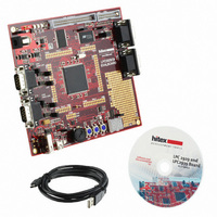
OM11027 NXP Semiconductors, OM11027 Datasheet - Page 67

OM11027
Manufacturer Part Number
OM11027
Description
BOARD EVAL LPC2939
Manufacturer
NXP Semiconductors
Type
MCUr
Datasheet
1.OM11027.pdf
(99 pages)
Specifications of OM11027
Contents
Board
For Use With/related Products
LPC2939
Lead Free Status / RoHS Status
Lead free / RoHS Compliant
Other names
568-4787
NXP Semiconductors
Table 34.
V
T
specified.
[1]
[2]
[3]
[4]
[5]
[6]
[7]
[8]
[9]
[10] The power-up reset has a time filter: V
LPC2939_3
Product data sheet
Symbol
I
I
I
Oscillator
V
R
C
Power-up reset
V
V
V
OL
OHS
OLS
vj
DD(CORE)
XIN_OSC
trip(high)
trip(low)
trip(dif)
s(xtal)
i
=
All parameters are guaranteed over the virtual junction temperature range by design. Pre-testing is performed at T
level. Cased products are tested at T
the specified temperature and power-supply voltage range.
Leakage current is exponential to temperature; worst-case value is at 85 C T
down.
V
V
Not 5 V-tolerant when pull-up is on.
For I/O Port 0, the maximum input voltage is defined by V
For Port 0, pin 0 to pin 15 add maximum 1.5 pF for input capacitance to ADC. For Port 0, pin 16 to pin 31 add maximum 1.0 pF for input
capacitance to ADC.
C
This parameter is not part of production testing or final testing, hence only a typical value is stated. Maximum and minimum values are
based on simulation results.
V
DDA(ADC3V3)
DDA(ADC5V0)
trip(low)
xtal
40
is crystal load capacitance and C
[1]
C to +85
= V
for 11 s before internal reset is asserted.
Static characteristics
DD(OSC_PLL)
Parameter
LOW-level output current
HIGH-level short-circuit
output current
LOW-level short-circuit
output current
voltage on pin XIN_OSC
crystal series resistance
input capacitance
high trip level voltage
low trip level voltage
difference between high
and low trip level voltage
must correlate with V
must correlate with V
C; all voltages are measured with respect to ground; positive currents flow into the IC; unless otherwise
; V
DD(IO)
= 2.7 V to 3.6 V; V
…continued
DDA(ADC5V0)
DDA(ADC3V3)
amb
ext
DD(CORE)
= 25 C (final testing). Both pre-testing and final testing use correlated test conditions to cover
are the two external load capacitors.
All information provided in this document is subject to legal disclaimers.
Conditions
at V
33 external series
resistor
at V
external series resistor
drive HIGH; pad
connected to ground
drive HIGH; pad
connected to V
f
f
of XIN_OSC
osc
osc
: V
: V
C
C
C
C
C
C
must be above V
OL
= 10 MHz to 15 MHz
xtal
ext
xtal
ext
= 15 MHz to 20 MHz
xtal
ext
OL
DDA(ADC3V3)
DDA(ADC5V0)
= 0.3 V; with 33
= 18 pF
= 39 pF
= 18 pF
= 0.3 V; without
= 10 pF;
= 20 pF;
= 10 pF;
Rev. 03 — 7 April 2010
DDA(ADC3V3)
I(ADC)
DD(IO)
= V
= V
.
DDA(ADC5V0)
DDA(ADC3V3)
trip(high)
= 3.0 V to 3.6 V; V
for 2 s before reset is de-asserted; V
ARM9 microcontroller with CAN, LIN, and USB
[10]
[10]
[10]
/ 1.5.
[8]
[8]
[9]
vj
1.5.
. All clocks off. Analog modules and FLASH powered
0
Min
26.7
5.0
-
-
-
-
-
-
1.1
1.0
50
DDA(ADC5V0)
Typ
-
-
-
-
-
-
-
-
-
1.4
1.3
120
= 3.0 V to 5.5 V;
Max
57.2
5.5
90.0
95.1
1.8
160
60
80
2
1.6
1.5
180
DD(CORE)
LPC2939
© NXP B.V. 2010. All rights reserved.
amb
= 85 C on wafer
must be below
67 of 99
Unit
mA
mA
mA
mA
V
pF
V
V
mV


