C8051F410DK Silicon Laboratories Inc, C8051F410DK Datasheet
C8051F410DK
Specifications of C8051F410DK
Available stocks


Related parts for C8051F410DK

C8051F410DK Summary of contents
Page 1
Analog Peripherals - 12-Bit ADC ±1 LSB INL; no missing codes • Programmable throughput up to 200 ksps • external inputs • Data dependent windowed interrupt generator • Built-in temperature sensor (±3 °C) • - Two 12-Bit ...
Page 2
C8051F410/1/2 OTES 2 Rev. 1.1 ...
Page 3
Table of Contents 1. System Overview.................................................................................................... 19 1.1. CIP-51™ Microcontroller................................................................................... 25 1.1.1. Fully 8051 Compatible Instruction Set...................................................... 25 1.1.2. Improved Throughput ............................................................................... 25 1.1.3. Additional Features .................................................................................. 25 1.2. On-Chip Debug Circuitry................................................................................... 26 1.3. On-Chip Memory............................................................................................... 27 1.4. Operating Modes ...
Page 4
C8051F410/1/2/3 10. CIP-51 Microcontroller ........................................................................................... 93 10.1.Instruction Set................................................................................................... 94 10.1.1.Instruction and CPU Timing ..................................................................... 94 10.1.2.MOVX Instruction and Program Memory ................................................. 95 10.2.Register Descriptions ....................................................................................... 98 10.3.Power Management Modes............................................................................ 101 10.3.1.Idle Mode ............................................................................................... 102 10.3.2.Stop Mode.............................................................................................. 102 10.3.3.Suspend Mode ....................................................................................... ...
Page 5
Data Storage .............................................................................. 137 16.3.Security Options ............................................................................................. 137 16.4.Flash Write and Erase Guidelines .................................................................. 139 16.4.1.VDD Maintenance and the VDD Monitor ............................................... 139 16.4.2.16.4.2 PSWE Maintenance .................................................................... 140 16.4.3.System Clock ......................................................................................... 140 16.5.Flash Read Timing ......................................................................................... 142 17. External ...
Page 6
C8051F410/1/2/3 21.3.3.SCL Low Timeout................................................................................... 194 21.3.4.SCL High (SMBus Free) Timeout .......................................................... 194 21.4.Using the SMBus............................................................................................ 194 21.4.1.SMBus Configuration Register............................................................... 195 21.4.2.SMB0CN Control Register ..................................................................... 198 21.4.3.Data Register ......................................................................................... 201 21.5.SMBus Transfer Modes.................................................................................. 201 21.5.1.Master Transmitter Mode ....................................................................... 201 21.5.2.Master Receiver ...
Page 7
Modules ............................................................................ 251 25.2.1.Edge-triggered Capture Mode................................................................ 252 25.2.2.Software Timer (Compare) Mode........................................................... 253 25.2.3.High Speed Output Mode....................................................................... 254 25.2.4.Frequency Output Mode ........................................................................ 255 25.2.5.8-Bit Pulse Width Modulator Mode......................................................... 256 25.2.6.16-Bit Pulse Width Modulator Mode....................................................... 257 25.3.Watchdog Timer Mode ................................................................................... 257 ...
Page 8
C8051F410/1/2 OTES 8 Rev. 1.1 ...
Page 9
List of Figures 1. System Overview Figure 1.1. C8051F410 Block Diagram .................................................................... 21 Figure 1.2. C8051F411 Block Diagram .................................................................... 22 Figure 1.3. C8051F412 Block Diagram .................................................................... 23 Figure 1.4. C8051F413 Block Diagram .................................................................... 24 Figure 1.5. Development/In-System Debug Diagram............................................... 26 ...
Page 10
C8051F410/1/2/3 Figure 9.3. Comparator Hysteresis Plot ................................................................... 85 10. CIP-51 Microcontroller Figure 10.1. CIP-51 Block Diagram.......................................................................... 93 11. Memory Organization and SFRs Figure 11.1. Memory Map ...................................................................................... 103 12. Interrupt Handler 13. Prefetch Engine 14. Cyclic Redundancy Check Unit (CRC0) ...
Page 11
Enhanced Serial Peripheral Interface (SPI0) Figure 23.1. SPI Block Diagram ............................................................................. 217 Figure 23.2. Multiple-Master Mode Connection Diagram ....................................... 220 Figure 23.3. 3-Wire Single Master and Slave Mode Connection Diagram ............. 220 Figure 23.4. 4-Wire Single Master and Slave ...
Page 12
C8051F410/1/2 OTES 12 Rev. 1.1 ...
Page 13
List of Tables 1. System Overview Table 1.1. Product Selection Guide ......................................................................... 20 Table 1.2. Operating Modes Summary .................................................................... 28 2. Absolute Maximum Ratings Table 2.1.Absolute Maximum Ratings . . . . . . . . . . . . ...
Page 14
C8051F410/1/2/3 17. External RAM 18. Port Input/Output Table 18.1.Port I/O DC Electrical Characteristics 163 19. Oscillators ...
Page 15
List of Registers SFR Definition 5.1. ADC0MX: ADC0 Channel Select . . . . . . . . . . . . . . . . . . . . . . . . . . 59 SFR Definition 5.2. ...
Page 16
C8051F410/1/2/3 SFR Definition 15.1. VDM0CN: VDD Monitor Control . . . . . . . . . . . . . . . . . . . . . . . . 130 SFR Definition 15.2. RSTSRC: Reset Source . ...
Page 17
SFR Definition 23.1. SPI0CFG: SPI0 Configuration . . . . . . . . . . . . . . . . . . . . . . . . . . 223 SFR Definition 23.2. SPI0CN: SPI0 Control . ...
Page 18
C8051F410/1/2 OTES 18 Rev. 1.1 ...
Page 19
System Overview C8051F41x devices are fully integrated, low power, mixed-signal system-on-a-chip MCUs. Highlighted fea- tures are listed below. Refer to Table 1.1 for specific product feature selection. • High-speed pipelined 8051-compatible microcontroller core ( MIPS) • In-system, ...
Page 20
C8051F410/1/2/3 Table 1.1. Product Selection Guide C8051F410- 2368 C8051F411- 2368 C8051F412- 2368 C8051F413- 2368 20 ...
Page 21
VREGIN VREG VDD (to smarRTClock Block) VRTC-BACKUP Battery Switch-Over Circuit (VDD >= VRTC-BACKUP) GND C2D Debug HW Reset /RST/C2CK Brown- POR Out External XTAL1 Oscillator Clock XTAL2 Circuit Mult. 24.5 MHz 2% Oscillator 32 KHz 64B ...
Page 22
C8051F410/1/2/3 (to rest of chip) VREGIN VREG VDD (to smaRTClock Block) VRTC-BACKUP Battery Switch-Over Circuit (VDD >= VRTC-BACKUP) GND C2D Debug HW /RST/C2CK Brown- POR Out External XTAL1 Oscillator Clock XTAL2 Circuit Mult. 24.5 MHz 2% Oscillator 32 KHz 64B ...
Page 23
VREGIN VREG VDD (to smaRTClocl Block) VRTC-BACKUP Battery Switch-Over Circuit (VDD >= VRTC-BACKUP) GND C2D Debug HW /RST/C2CK Brown- POR Out External XTAL1 Oscillator Clock XTAL2 Circuit Mult. 24.5 MHz 2% Oscillator 32 KHz 64B RAM ...
Page 24
C8051F410/1/2/3 (to rest of chip) VREGIN VREG VDD (to smaRTClock Block) VRTC-BACKUP Battery Switch-Over Circuit (VDD >= VRTC-BACKUP) GND C2D Debug HW /RST/C2CK Brown- POR Out External XTAL1 Oscillator Clock XTAL2 Circuit Mult. 24.5 MHz 2% Oscillator 32 KHz 64B ...
Page 25
CIP-51™ Microcontroller 1.1.1. Fully 8051 Compatible Instruction Set The C8051F41x devices use Silicon Laboratories’ proprietary CIP-51 microcontroller core. The CIP-51 is fully compatible with the MCS-51™ instruction set. Standard 803x/805x assemblers and compilers can be used to develop software. ...
Page 26
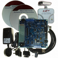
... All the peripherals (except for the ADC and SMBus) are stalled when the MCU is halted, during single stepping breakpoint in order to keep them synchronized. The C8051F410DK development kit provides all the hardware and software necessary to develop applica- tion code and perform in-circuit debugging with the C8051F41x MCUs. The kit includes software with a developer's studio and debugger, a USB debug adapter, a target application board with the associated MCU installed, and the required cables and wall-mount power supply ...
Page 27
On-Chip Memory The CIP-51 has a standard 8051 program and data address configuration. It includes 256 bytes of data RAM, with the upper 128 bytes dual-mapped. Indirect addressing accesses the upper 128 bytes of general purpose RAM, and direct ...
Page 28
C8051F410/1/2/3 1.4. Operating Modes The C8051F41x devices have four operating modes: Active (Normal), Idle, Suspend, and Stop. Active mode occurs during normal operation when the oscillator and peripherals are active. Idle mode halts the CPU while leaving the peripherals and ...
Page 29
Analog to Digital Converter The C8051F41x devices include an on-chip 12-bit SAR ADC with a 27-channel single-ended input multi- plexer and a maximum throughput of 200 ksps. The ADC system includes a configurable analog multi- plexer that selects ...
Page 30
C8051F410/1/2/3 Data Write Timer 0 Timer 1 Timer 2 Timer 3 CNVSTR 12-bit Digital Input 12-bit Digital Input Data Write Timer 0 Timer 1 Timer 2 Timer 3 CNVSTR Figure 1.8. IDAC Block Diagram 1.7. Programmable Comparators C8051F41x devices include ...
Page 31
Port I/O Pins Port I/O Pins Figure 1.9. Comparators Block Diagram 1.8. Cyclic Redundancy Check Unit C8051F41x devices include a cyclic redundancy check unit (CRC0) that can perform a CRC using a 16-bit or 32-bit polynomial. CRC0 accepts a stream ...
Page 32
C8051F410/1/2/3 1.11. smaRTClock (Real Time Clock) C8051F41x devices include a smaRTClock Peripheral (Real Time Clock). The smaRTClock has a dedi- cated 32 kHz oscillator that can be configured for use with or without a crystal, a 47-bit smaRTClock timer with ...
Page 33
Port Input/Output C8051F41x devices include I/O pins. Port pins are organized as three byte-wide ports. The port pins behave like typical 8051 ports with a few enhancements. Each port pin can be configured as a digital ...
Page 34
C8051F410/1/2/3 1.13. Programmable Counter Array The Programmable Counter Array (PCA0) provides enhanced timer functionality while requiring less CPU intervention than the standard 8051 counter/timers. The PCA consists of a dedicated 16-bit counter/timer and six 16-bit capture/compare modules. The counter/timer is ...
Page 35
Absolute Maximum Ratings Table 2.1. Absolute Maximum Ratings* Parameter Ambient temperature under bias Storage Temperature Voltage on V with respect to GND REGIN Voltage on V with respect to GND DD Voltage on V with respect to GND RTC-BACKUP ...
Page 36
C8051F410/1/2/3 3. Global DC Electrical Characteristics Table 3.1. Global DC Electrical Characteristics –40 to +85 °C, 50 MHz System Clock unless otherwise specified. Typical values are given at 25 °C Parameter 1 Supply Input Voltage (V ) REGIN Core Supply ...
Page 37
Table 3.1. Global DC Electrical Characteristics (Continued) –40 to +85 °C, 50 MHz System Clock unless otherwise specified. Typical values are given at 25 °C Parameter Digital Supply Current—CPU Active (Normal Mode, fetching instructions from Flash) 6 Core Supply Current ...
Page 38
C8051F410/1/2/3 Table 3.1. Global DC Electrical Characteristics (Continued) –40 to +85 °C, 50 MHz System Clock unless otherwise specified. Typical values are given at 25 °C Parameter Digital Supply Current—CPU Inactive (Idle Mode, not fetching instructions from Flash) 6 Core ...
Page 39
Table 3.2. Index to Electrical Characteristics Tables Table Title ADC0 Electrical Characteristics (VDD = 2.5 V, VREF = 2.2 V) ADC0 Electrical Characteristics (VDD = 2.1 V, VREF = 1.5 V) IDAC Electrical Characteristics Voltage Reference Electrical Characteristics Voltage Regulator ...
Page 40
C8051F410/1/2 OTES 40 Rev. 1.1 ...
Page 41
Pinout and Package Definitions Table 4.1. Pin Definitions for the C8051F41x Pin Numbers Name ‘F410/2 ‘F411 GND RTC-BACKUP REGIN RST C2CK ...
Page 42
C8051F410/1/2/3 Table 4.1. Pin Definitions for the C8051F41x (Continued) Pin Numbers Name ‘F410/2 ‘F411/3 P0. P0. P0. CNVSTR P0 P1. XTAL1 P1. XTAL2 P1 ...
Page 43
Table 4.1. Pin Definitions for the C8051F41x (Continued) Pin Numbers Name ‘F410/2 ‘F411 P2.3* 28 P2.4* 29 P2.5* 30 P2.6* 31 *Note: Available only on the C8051F410/2. C8051F410/1/2/3 ...
Page 44
C8051F410/1/2 RST/C2CK RTC-BACKUP XTAL4 4 XTAL3 5 6 GND REGIN Figure 4.1. LQFP-32 Pinout Diagram (Top View) 44 C8051F410/2 Top View Rev. 1.1 24 P0.7 23 P0.6 / CNVSTR ...
Page 45
RST / C2CK RTC-BACKUP XTAL4 3 XTAL3 4 GND REGIN Figure 4.2. QFN-28 Pinout Diagram (Top View) C8051F410/1/2/3 C8051F411/3 Top View GND Rev. 1 P0.4 / ...
Page 46
C8051F410/1/2/3 Figure 4.3. LQFP-32 Package Diagram Table 4.2. LQFP-32 Package Dimensions MIN TYP MAX — — 1.60 0.05 — 0.15 1.35 1.40 1.45 0.30 0.37 0.45 0.09 ...
Page 47
Figure 4.4. LQFP-32 Recommended PCB Land Pattern Table 4.3. LQFP-32 PCB Land Pattern Dimensions Dimension Min C1 8. 0.40 Y1 1.25 Rev. 1.1 C8051F410/1/2/3 Max 8.50 8.50 0.80 BSC 0.50 1.35 47 ...
Page 48
C8051F410/1/2/3 Figure 4.5. QFN-28 Package Drawing Table 4.4. QFN-28 Package Dimensions Dimension Min Typ A 0.80 0.90 A1 0.00 0.02 A3 0.25 REF b 0.18 0.23 D 5.00 BSC. D2 2.90 3.15 e 0.50 BSC. E 5.00 BSC. E2 2.90 ...
Page 49
Figure 4.6. QFN-28 Recommended PCB Land Pattern Table 4.5. QFN-28 PCB Land Pattern Dimensions Dimension Min Max C1 4.80 C2 4.80 E 0.50 X1 0.20 0.30 Notes: General 1. All dimensions shown are in millimeters (mm) unless otherwise noted. 2. ...
Page 50
C8051F410/1/2 OTES 50 Rev. 1.1 ...
Page 51
ADC (ADC0) The ADC0 subsystem for the C8051F41x consists of an analog multiplexer (AMUX0) with 27 total input selections, and a 200 ksps, 12-bit successive-approximation-register ADC with integrated track-and-hold, programmable window detector, and hardware accumulator. The ADC0 subsystem ...
Page 52
C8051F410/1/2/3 5.2. Temperature Sensor The typical temperature sensor transfer function is shown in Figure 5.2. The output voltage (V positive ADC input when the temperature sensor is selected by bits AD0MX4-0 in register ADC0MX. (Volts) 1.000 0.900 0.800 0.700 0.600 ...
Page 53
Starting a Conversion A conversion can be initiated in one of four ways, depending on the programmed states of the ADC0 Start of Conversion Mode bits (AD0CM1-0) in register ADC0CN. Conversions may be initiated by one of the fol- ...
Page 54
C8051F410/1/2/3 Depending on the output connected to the ADC input, additional tracking time, more than is specified in Table 5.3 and Table 5.4, may be required after changing MUX settings. See the settling time requirements described in Section “5.3.6. Settling ...
Page 55
Convert Start Time ADC0 State AD0INT Flag Post-Tracking or Dual-Tracking Modes (AD0TK = ‘00') Time ADC0 State Track AD0INT Flag Key F Equal to one period of FCLK. Each Sn is equal to one ...
Page 56
C8051F410/1/2/3 5.3.4. Burst Mode Burst Mode is a power saving feature that allows ADC0 to remain in a low power state between conver- sions. When Burst Mode is enabled, ADC0 wakes from a low power state, accumulates ...
Page 57
Output Conversion Code The registers ADC0H and ADC0L contain the high and low bytes of the output conversion code. When the repeat count is set to 1, conversion codes are represented in 12-bit unsigned integer format and the output ...
Page 58
C8051F410/1/2/3 5.3.6. Settling Time Requirements A minimum tracking time is required before an accurate conversion can be performed. This tracking time is determined by the AMUX0 resistance, the ADC0 sampling capacitance, any external source resistance, and the accuracy required for ...
Page 59
SFR Definition 5.1. ADC0MX: ADC0 Channel Select Bit7 Bit6 Bit5 Bits7–5: UNUSED. Read = 000b; Write = don’t care. Bits4–0: AD0MX4–0: AMUX0 Positive Input Selection AD0MX4–0 00000 00001 00010 00011 00100 00101 00110 00111 ...
Page 60
C8051F410/1/2/3 SFR Definition 5.2. ADC0CF: ADC0 Configuration R/W R/W R/W AD0SC Bit7 Bit6 Bit5 Bits7–3: AD0SC4–0: ADC0 SAR Conversion Clock Period Bits. SAR Conversion clock is derived from FCLK by the following equation, where AD0SC refers to the 5-bit value ...
Page 61
SFR Definition 5.3. ADC0H: ADC0 Data Word MSB R/W R/W R/W Bit7 Bit6 Bit5 ADC0 Data Word High-Order Bits. Bits7-0: For AD0LJST = 0 and AD0RPT as follows: 00: Bits 3–0 are the upper 4 bits of the accumulated ...
Page 62
C8051F410/1/2/3 SFR Definition 5.5. ADC0CN: ADC0 Control R/W R/W R/W AD0EN BURSTEN AD0INT AD0BUSY AD0WINT AD0LJST AD0CM1 AD0CM0 00000000 Bit7 Bit6 Bit5 Bit7: AD0EN: ADC0 Enable Bit. 0: ADC0 Disabled. ADC0 is in low-power shutdown. 1: ADC0 Enabled. ADC0 is ...
Page 63
SFR Definition 5.6. ADC0TK: ADC0 Tracking Mode Select R/W R/W R/W AD0PWR Bit7 Bit6 Bit5 Bits7–4: AD0PWR3–0: ADC0 Burst Power-Up Time. For BURSTEN = 0: ADC0 power state controlled by AD0EN. For BURSTEN = 1 and AD0EN = 1; ADC0 ...
Page 64
C8051F410/1/2/3 SFR Definition 5.7. ADC0GTH: ADC0 Greater-Than Data High Byte R/W R/W R/W Bit7 Bit6 Bit5 Bits7–0: High byte of ADC0 Greater-Than Data Word. SFR Definition 5.8. ADC0GTL: ADC0 Greater-Than Data Low Byte R/W R/W R/W Bit7 Bit6 Bit5 Bits7–0: ...
Page 65
SFR Definition 5.9. ADC0LTH: ADC0 Less-Than Data High Byte R/W R/W R/W Bit7 Bit6 Bit5 Bits7–0: High byte of ADC0 Less-Than Data Word. SFR Definition 5.10. ADC0LTL: ADC0 Less-Than Data Low Byte R/W R/W R/W Bit7 Bit6 Bit5 Bits7–0: Low ...
Page 66
C8051F410/1/2/3 5.4.1. Window Detector In Single-Ended Mode Figure 5.7 shows two example ADC0LTH:ADC0LTL = 0x0200 (512d) and ADC0GTH:ADC0GTL = 0x0100 (256d). The input voltage can range from ‘0’ (4095/4096) with respect to GND, and is represented by ...
Page 67
Table 5.3. ADC0 Electrical Characteristics ( 2 2.2 V (REFSL=0), –40 to +85 °C unless otherwise specified. Typical values are given DD REF at 25 ºC. Parameter DC Accuracy Resolution Integral Nonlinearity Differential Nonlinearity Guaranteed ...
Page 68
C8051F410/1/2/3 Table 5.4. ADC0 Electrical Characteristics ( 2 1.5 V (REFSL = 0), –40 to +85 °C unless otherwise specified. DD REF 25 ºC. Parameter DC Accuracy Resolution Integral Nonlinearity Differential Nonlinearity Guaranteed Monotonic Offset ...
Page 69
Current Mode DACs (IDA0 and IDA1) The C8051F41x devices include two 12-bit current-mode Digital-to-Analog Converters (IDACs). The maxi- mum current output of the IDACs can be adjusted for four different current settings; 0.25 mA, 0.5 mA, 1 mA, ...
Page 70
C8051F410/1/2/3 6.1.2. Update Output Based on Timer Overflow The IDAC output update can be scheduled on a Timer overflow. This feature is useful in systems where the IDAC is used to generate a waveform of a defined sampling rate, by ...
Page 71
SFR Definition 6.1. IDA0CN: IDA0 Control R/W R/W R/W IDA0EN IDA0CM Bit7 Bit6 Bit5 Bit 7: IDA0EN: IDA0 Enable Bit. 0: IDA0 Disabled. 1: IDA0 Enabled. Bits 6–4: IDA0CM[2:0]: IDA0 Update Source Select Bits. 000: DAC output updates on Timer ...
Page 72
C8051F410/1/2/3 SFR Definition 6.3. IDA0L: IDA0 Data Low Byte R/W R/W R/W Bit7 Bit6 Bit5 Bits 7–0: IDA0 Data Word Low-Order Bits. For IDA0RJST = 0: Bits 7-4 hold the least significant 4-bits of the 12-bit IDA0 Data Word. Bits ...
Page 73
SFR Definition 6.5. IDA1H: IDA0 Data High Byte R/W R/W R/W Bit7 Bit6 Bit5 Bits 7–0: IDA1 Data Word High-Order Bits. For IDA0RJST = 0: Bits 7-0 hold the most significant 8-bits of the 12-bit IDA1 Data Word. For IDA0RJST ...
Page 74
C8051F410/1/2/3 IDA0 IDA1 Figure 6.3. IDAC Pin Connections 74 IDA0EN 0 P0.0 1 IDA1EN IDAMRG Rev. 1.1 ...
Page 75
Table 6.1. IDAC Electrical Characteristics –40 to +85 ° 2.0 V Full-scale output current set unless otherwise specified. Typical values are given ºC. Parameter Static Performance Resolution Integral Nonlinearity Differential Nonlinearity Guaranteed ...
Page 76
C8051F410/1/2 OTES 76 Rev. 1.1 ...
Page 77
Voltage Reference The Voltage reference MUX on C8051F41x devices is configurable to use an externally connected voltage reference, the internal reference voltage generator, or the V REFSL bit in the Reference Control register (REF0CN) selects the reference source. For ...
Page 78
C8051F410/1/2/3 Important Note About the V Pin: Port pin P1.2 is used as the external V REF the internal V . When using either an external voltage reference or the internal reference circuitry, P1.2 REF should be configured as an ...
Page 79
Table 7.1. Voltage Reference Electrical Characteristics V = 2.0 V; –40 to +85 °C unless otherwise specified. DD Parameter Internal Reference (REFBE = 1) 25 °C ambient (REFLV = 0) Output Voltage 25 °C ambient (REFLV = 1 ...
Page 80
C8051F410/1/2 OTES 80 Rev. 1.1 ...
Page 81
Voltage Regulator (REG0) C8051F41x devices include an on-chip low dropout voltage regulator (REG0). The input to REG0 at the V pin can be as high as 5.25 V. The output can be selected by software to 2 ...
Page 82
C8051F410/1/2/3 SFR Definition 8.1. REG0CN: Regulator Control R/W R/W R REGDIS Reserved — Bit7 Bit6 Bit5 Bit 7: REGDIS: Voltage Regulator Disable Bit. This bit disables/enables the Voltage Regulator. 0: Voltage Regulator Enabled. 1: Voltage Regulator Disabled. Bit 6: RESERVED. ...
Page 83
Comparators C8051F41x devices include two on-chip programmable voltage comparators: Comparator0 is shown in Figure 9.1; Comparator1 is shown in Figure 9.2. The two comparators operate identically, but only Comparator0 can be used as a reset source. The Comparator offers ...
Page 84
C8051F410/1/2/3 The Comparator output can be polled in software, used as an interrupt source, internal oscillator suspend awakening source and/or routed to a Port pin. When routed to a Port pin, the Comparator output is avail- able asynchronous or synchronous ...
Page 85
CP0+ VIN+ + CP0 CP0- _ VIN- CIRCUIT CONFIGURATION Positive Hysteresis Voltage (Programmed with CP0HYP Bits) VIN- INPUTS VIN OUTPUT V OL Positive Hysteresis Disabled Figure 9.3. Comparator Hysteresis Plot The Comparator hysteresis is software-programmable via its Comparator ...
Page 86
C8051F410/1/2/3 SFR Definition 9.1. CPT0CN: Comparator0 Control R/W R R/W CP0EN CP0OUT CP0RIF Bit7 Bit6 Bit5 Bit7: CP0EN: Comparator0 Enable Bit. 0: Comparator0 Disabled. 1: Comparator0 Enabled. Bit6: CP0OUT: Comparator0 Output State Flag. 0: Voltage on CP0+ < CP0–. 1: ...
Page 87
SFR Definition 9.2. CPT0MX: Comparator0 MUX Selection R/W R/W R/W CMX0N3 CMX0N2 CMX0N1 CMX0N0 CMX0P3 CMX0P2 CMX0P1 CMX0P0 Bit7 Bit6 Bit5 Bits7–4: CMX0N3–CMX0N0: Comparator0 Negative Input MUX Select. These bits select which Port pin is used as the Comparator0 negative ...
Page 88
C8051F410/1/2/3 SFR Definition 9.3. CPT0MD: Comparator0 Mode Selection R/W R/W R/W RESERVED - CP0RIE Bit7 Bit6 Bit5 Bit7: RESERVED. Read = 0b. Must Write 0b. Bit6: UNUSED. Read = 0b. Write = don’t care. Bit5: CP0RIE: Comparator Rising-Edge Interrupt Enable. ...
Page 89
SFR Definition 9.4. CPT1MX: Comparator1 MUX Selection R/W R/W R/W CMX1N3 CMX1N2 CMX1N1 CMX1N0 CMX1P3 CMX1P2 CMX1P1 CMX1P0 Bit7 Bit6 Bit5 Bits7–4: CMX1N3–CMX1N0: Comparator1 Negative Input MUX Select. These bits select which Port pin is used as the Comparator1 negative ...
Page 90
C8051F410/1/2/3 SFR Definition 9.5. CPT1MD: Comparator1 Mode Selection R/W R/W R/W RESERVED - CP1RIE Bit7 Bit6 Bit5 Bit7: RESERVED. Read = 0b. Must Write 0b. Bit6: UNUSED. Read = 0b. Write = don’t care. Bit5: CP1RIE: Comparator Rising-Edge Interrupt Enable. ...
Page 91
SFR Definition 9.6. CPT1CN: Comparator1 Control R/W R R/W CP1EN CP1OUT CP1RIF Bit7 Bit6 Bit5 Bit7: CP1EN: Comparator1 Enable Bit. 0: Comparator1 Disabled. 1: Comparator1 Enabled. Bit6: CP1OUT: Comparator1 Output State Flag. 0: Voltage on CP1+ < CP1-. 1: Voltage ...
Page 92
C8051F410/1/2/3 Table 9.1. Comparator Electrical Characteristics V = 2.0 V, –40 to +85 °C unless otherwise noted. All specifications apply to both Comparator0 and Comparator1 DD unless otherwise noted. Typical values are given at 25 ºC. Parameter Response Time: 1 ...
Page 93
CIP-51 Microcontroller The MCU system controller core is the CIP-51 microcontroller. The CIP-51 is fully compatible with the MCS-51™ instruction set. Standard 803x/805x assemblers and compilers can be used to develop soft- ware. The C8051F41x family has a superset ...
Page 94
C8051F410/1/2/3 Performance The CIP-51 employs a pipelined architecture that greatly increases its instruction throughput over the stan- dard 8051 architecture standard 8051, all instructions except for MUL and DIV take system clock cycles to execute, ...
Page 95
MOVX Instruction and Program Memory The MOVX instruction is typically used to access data stored in XDATA memory space. In the CIP-51, the MOVX instruction can also be used to write or erase on-chip program memory space implemented as ...
Page 96
C8051F410/1/2/3 Table 10.1. CIP-51 Instruction Set Summary Mnemonic ORL A, @Ri OR indirect RAM to A ORL A, #data OR immediate to A ORL direct direct byte ORL direct, #data OR immediate to direct byte XRL ...
Page 97
Table 10.1. CIP-51 Instruction Set Summary Mnemonic POP direct Pop direct byte from stack XCH A, Rn Exchange Register with A XCH A, direct Exchange direct byte with A XCH A, @Ri Exchange indirect RAM with A XCHD A, @Ri ...
Page 98
C8051F410/1/2/3 Notes on Registers, Operands and Addressing Modes Register R0-R7 of the currently selected register bank. @Ri - Data RAM location addressed indirectly through R0 or R1. rel - 8-bit, signed (two’s complement) offset relative to the first ...
Page 99
SFR Definition 10.2. DPL: Data Pointer Low Byte R/W R/W R/W Bit7 Bit6 Bit5 Bits7–0: DPL: Data Pointer Low. The DPL register is the low byte of the 16-bit DPTR. DPTR is used to access indirectly addressed XRAM and Flash ...
Page 100
C8051F410/1/2/3 SFR Definition 10.4. PSW: Program Status Word R/W R/W R Bit7 Bit6 Bit5 Bit7: CY: Carry Flag. This bit is set when the last arithmetic operation resulted in a carry (addition borrow (subtraction). It ...
Page 101
SFR Definition 10.5. ACC: Accumulator R/W R/W R/W ACC.7 ACC.6 ACC.5 Bit7 Bit6 Bit5 Bits7–0: ACC: Accumulator. This register is the accumulator for arithmetic operations. SFR Definition 10. Register R/W R/W R/W B.7 B.6 B.5 Bit7 Bit6 Bit5 ...
Page 102
C8051F410/1/2/3 10.3.1. Idle Mode Setting the Idle Mode Select bit (PCON.0) causes the CIP-51 to halt the CPU and enter Idle mode as soon as the instruction that sets the bit completes execution. All internal registers and memory maintain their ...
Page 103
Memory Organization and SFRs The memory organization of the C8051F41x is similar to that of a standard 8051. There are two separate memory spaces: program memory and data memory. Program and data memory share the same address space but ...
Page 104
C8051F410/1/2/3 11.2. Data Memory The C8051F41x includes 256 bytes of internal RAM mapped into the data memory space from 0x00 through 0xFF. The lower 128 bytes of data memory are used for general purpose registers and scratch pad memory. Either ...
Page 105
Special Function Registers The direct-access data memory locations from 0x80 to 0xFF constitute the special function registers (SFRs). The SFRs provide control and data exchange with the CIP-51's resources and peripherals. The CIP-51 duplicates the SFRs found in a ...
Page 106
C8051F410/1/2/3 Table 11.2. Special Function Registers SFRs are listed in alphabetical order. All undefined SFR locations are reserved. Register Address ACC 0xE0 Accumulator ADC0CF 0xBC ADC0 Configuration ADC0CN 0xE8 ADC0 Control ADC0H 0xBE ADC0 ADC0L 0xBD ADC0 ADC0GTH 0xC4 ADC0 ...
Page 107
Table 11.2. Special Function Registers (Continued) SFRs are listed in alphabetical order. All undefined SFR locations are reserved. Register Address IDA1L 0xF4 Current Mode DAC1 Low Byte IDA1CN 0xB5 Current Mode DAC1 Control IE 0xA8 Interrupt Enable IP 0xB8 Interrupt ...
Page 108
C8051F410/1/2/3 Table 11.2. Special Function Registers (Continued) SFRs are listed in alphabetical order. All undefined SFR locations are reserved. Register Address PCA0CPL5 0xD2 PCA Capture 5 Low PCA0CPM0 0xDA PCA Module 0 Mode PCA0CPM1 0xDB PCA Module 1 Mode PCA0CPM2 ...
Page 109
Table 11.2. Special Function Registers (Continued) SFRs are listed in alphabetical order. All undefined SFR locations are reserved. Register Address TMR2L 0xCC Timer/Counter 2 Low TMR2RLH 0xCB Timer/Counter 2 Reload High TMR2RLL 0xCA Timer/Counter 2 Reload Low TMR3CN 0x91 Timer/Counter ...
Page 110
C8051F410/1/2/3 12. Interrupt Handler The C8051F41x family includes an extended interrupt system supporting a total of 18 interrupt sources with two priority levels. The allocation of interrupt sources between on-chip peripherals and external input pins varies according to the specific ...
Page 111
In this case, the response time is 19 system clock cycles: 1 clock cycle to detect the interrupt, 5 clock cycles to execute the RETI, 8 clock cycles to complete the DIV instruction and 5 clock cycles to exe- ...
Page 112
C8051F410/1/2/3 12.4. Interrupt Register Descriptions The SFRs used to enable the interrupt sources and set their priority level are described below. Refer to the data sheet section associated with a particular on-chip peripheral for information regarding valid interrupt conditions for ...
Page 113
SFR Definition 12.2. IP: Interrupt Priority R R/W R/W - PSPI0 PT2 Bit7 Bit6 Bit5 Bit 7: UNUSED. Read = 1, Write = don't care. Bit 6: PSPI0: Serial Peripheral Interface (SPI0) Interrupt Priority Control. This bit sets the priority ...
Page 114
C8051F410/1/2/3 SFR Definition 12.3. EIE1: Extended Interrupt Enable 1 R/W R/W R/W ET3 ECP1 ECP0 Bit7 Bit6 Bit5 Bit 7: ET3: Enable Timer 3 Interrupt. This bit sets the masking of the Timer 3 interrupt. 0: Disable Timer 3 interrupts. ...
Page 115
SFR Definition 12.4. EIP1: Extended Interrupt Priority 1 R/W R/W R/W PT3 PCP1 PCP0 Bit7 Bit6 Bit5 Bit 7: PT3: Timer 3 Interrupt Priority Control. This bit sets the priority of the Timer 3 interrupt. 0: Timer 3 interrupts set ...
Page 116
C8051F410/1/2/3 SFR Definition 12.5. EIE2: Extended Interrupt Enable 2 R/W R/W R Bit7 Bit6 Bit5 Bits 7–2: UNUSED. Read = 000000b. Write = don’t care. Bit 1: EMAT: Enable Port Match Interrupt. This bit sets the masking ...
Page 117
External Interrupts The /INT0 and /INT1 external interrupt sources are configurable as active high or low, edge or level sensi- tive. The IN0PL (/INT0 Polarity) and IN1PL (/INT1 Polarity) bits in the IT01CF register select active high or active ...
Page 118
C8051F410/1/2/3 SFR Definition 12.7. IT01CF: INT0/INT1 Configuration R/W R/W R/W IN1PL IN1SL2 IN1SL1 Bit7 Bit6 Bit5 Note: Refer to SFR Definition 24.1. “TCON: Timer Control” on page 235 for INT0/1 edge- or level-sensitive interrupt selection. Bit 7: IN1PL: /INT1 Polarity ...
Page 119
Prefetch Engine The C8051F41x family of devices incorporate a 2-byte prefetch engine. Due to Flash access time specifi- cations, the prefetch engine is necessary for full-speed (50 MHz) code execution. Instructions are read from Flash memory two bytes at ...
Page 120
C8051F410/1/2 OTES 120 Rev. 1.1 ...
Page 121
Cyclic Redundancy Check Unit (CRC0) C8051F41x devices include a cyclic redundancy check unit (CRC0) that can perform a CRC using a 16-bit or 32-bit polynomial. CRC0 accepts a stream of 8-bit data written to the CRC0IN register. CRC0 posts ...
Page 122
C8051F410/1/2/3 For example, the 16-bit 'F41x CRC algorithm can be described by the following code: unsigned short UpdateCRC (unsigned short CRC_acc, unsigned char CRC_input) { unsigned char i; #define POLY 0x1021 // Create the CRC "dividend" for polynomial arithmetic (binary ...
Page 123
CRC Algorithm The C8051F41x CRC unit calculates the 32-bit CRC using a poly of 0x04C11DB7. The CRC-32 algorithm is "reflected", meaning that all of the input bytes and the final 32-bit output are bit-reversed in the process- ing ...
Page 124
C8051F410/1/2/3 Table 14.2. Example 32-bit CRC Outputs Input 0x63 0xAA, 0xBB, 0xCC 0x00, 0x00, 0xAA, 0xBB, 0xCC 14.3. Preparing for a CRC Calculation To prepare CRC0 for a CRC calculation, software should select the desired polynomial and set the initial ...
Page 125
SFR Definition 14.1. CRC0CN: CRC0 Control CRC0SEL CRC0INIT CRC0VAL Bit7 Bit6 Bit5 Bits 7–5: UNUSED. Read = 0b. Write = don’t care. Bit 4: CRC0SEL: CRC0 Polynomial Select Bit. 0: CRC0 uses the 32-bit ...
Page 126
C8051F410/1/2/3 SFR Definition 14.3. CRC0DAT: CRC0 Data Output R/W R/W R/W Bit7 Bit6 Bit5 Bits 7–0: CRC0DAT: Indirect CRC Result Data Bits. Each operation performed on CRC0DAT targets the CRC result bits pointed to by CRC0PNT. SFR Definition 14.4. CRC0FLIP: ...
Page 127
Reset Sources Reset circuitry allows the controller to be easily placed in a predefined default condition. On entry to this reset state, the following occur: • CIP-51 halts program execution • Special Function Registers (SFRs) are initialized to their ...
Page 128
C8051F410/1/2/3 15.1. Power-On Reset During power-up, the device is held in a reset state and the RST pin is driven low until additional delay occurs before the device is released from reset; the delay decreases as ...
Page 129
Power-Fail Reset / V DD When the VDD Monitor is selected as a reset source and a power-down transition or power irregularity causes V to drop below V , the power supply monitor will drive the RST pin low ...
Page 130
C8051F410/1/2/3 SFR Definition 15.1. VDM0CN: V R/W R R/W VDMEN VDDSTAT VDMLVL Reserved Reserved Reserved Reserved Reserved 1v000000 Bit7 Bit6 Bit5 Bit7: VDMEN: V Monitor Enable. DD This bit turns the V monitor circuit on/off. The V DD until it ...
Page 131
CP0+) is less than the inverting input voltage (on CP0-), the device is put into the reset state. After a Comparator0 reset, the C0RSEF flag (RSTSRC.5) will read ‘1’ signifying Comparator0 as the reset source; otherwise, ...
Page 132
C8051F410/1/2/3 15.8. smaRTClock (Real Time Clock) Reset The smaRTClock can generate a system reset on two events: smaRTClock Oscillator Fail or smaRTClock Alarm. The smaRTClock Oscillator Fail event occurs when the smaRTClock Missing Clock Detector is enabled and the smaRTClock ...
Page 133
SFR Definition 15.2. RSTSRC: Reset Source R/W R R/W RTC0RE FERROR C0RSEF SWRSF Bit7 Bit6 Bit5 Note: For bits that act as both reset source enables (on a write) and reset indicator flags (on a read), read-modify-write instructions read and ...
Page 134
C8051F410/1/2/3 Table 15.1. Reset Electrical Characteristics –40 to +85 °C unless otherwise specified. Typical values are given at 25 ºC. Parameter RST Output Low Voltage RST Input High Voltage RST Input Low Voltage RST Input Pullup Impedance V Monitor Threshold ...
Page 135
Flash Memory On-chip, re-programmable Flash memory is included for program code and non-volatile data storage. The Flash memory can be programmed in-system through the C2 interface or by software using the MOVX write instruction. Once cleared to logic 0, ...
Page 136
C8051F410/1/2/3 16.1.3. Flash Write Procedure Bytes in Flash memory can be written one byte at a time groups of two. The FLBWE bit in register PFE0CN (SFR Definition 13.1) controls whether a single byte or a block of ...
Page 137
Non-volatile Data Storage The Flash memory can be used for non-volatile data storage as well as program code. This allows data such as calibration coefficients to be calculated and stored at run time. Data is written using the MOVX ...
Page 138
C8051F410/1/2/3 The level of Flash security depends on the Flash access method. The three Flash access methods that can be restricted are reads, writes, and erases from the C2 debug interface, user firmware executing on unlocked pages, and user firmware ...
Page 139
Flash Write and Erase Guidelines Any system which contains routines which write or erase Flash memory from software involves some risk that the write or erase routines will execute unintentionally if the CPU is operating outside its specified operating ...
Page 140
C8051F410/1/2/3 16.4.2. 16.4.2 PSWE Maintenance 7. Reduce the number of places in code where the PSWE bit (b0 in PSCTL) is set to a '1'. There should be exactly one routine in code that sets PSWE to a '1' to ...
Page 141
SFR Definition 16.1. PSCTL: Program Store R/W Control Bit7 Bit6 Bit5 Bits7–2: UNUSED: Read = 000000b, Write = don’t care. Bit1: PSEE: Program Store Erase Enable Setting this bit (in combination with PSWE) allows ...
Page 142
C8051F410/1/2/3 16.5. Flash Read Timing On reset, the C8051F41x Flash read timing is configured for operation with system clocks MHz. If the system clock will not be increased above 25 MHz, then the Flash timing registers may ...
Page 143
SFR Definition 16.4. ONESHOT: Flash Oneshot Period Bit7 Bit6 Bit5 Bits7–4: UNUSED. Read = 0000b. Write = don’t care. Bits3–0: PERIOD: Oneshot Period Control Bits. These bits limit the internal Flash read strobe width ...
Page 144
C8051F410/1/2 OTES 144 Rev. 1.1 ...
Page 145
External RAM The C8051F41x devices include 2048 bytes of RAM mapped into the external data memory space. All of these address locations may be accessed using the external move instruction (MOVX) and the data pointer (DPTR), or using MOVX ...
Page 146
C8051F410/1/2 OTES 146 Rev. 1.1 ...
Page 147
Port Input/Output Digital and analog resources are available through I/O pins. Port pins are organized as three byte- wide Ports. Each of the Port pins can be defined as general-purpose I/O (GPIO) or analog input/output; Port ...
Page 148
C8051F410/1/2/3 /WEAK-PULLUP PUSH-PULL /PORT-OUTENABLE PORT-OUTPUT Analog Select ANALOG INPUT PORT-INPUT Figure 18.2. Port I/O Cell Block Diagram 148 VIO VIO (WEAK) GND Rev. 1.1 PORT PAD ...
Page 149
Priority Crossbar Decoder The Priority Crossbar Decoder (Figure 18.3) assigns a priority to each I/O function, starting at the top with UART0. When a digital resource is selected, the least-significant unassigned Port pin is assigned to that resource (excluding ...
Page 150
C8051F410/1/2 Signa PIN I TX0 RX0 SCK MISO MOSI NSS* SDA SCL CP0 CP0A CP1 CP1A /SYSCLK CEX0 CEX1 CEX2 CEX3 CEX4 CEX5 ECI ...
Page 151
Port I/O Initialization Port I/O initialization consists of the following steps: Step 1. Select the input mode (analog or digital) for all Port pins, using the Port Input Mode register (PnMDIN). If the pin is in analog mode, a ...
Page 152
C8051F410/1/2 P0.x I Vtest pin I/O Cell + - Figure 18.5. Port 0 Input Overdrive Current Range The output driver characteristics of the I/O pins are defined using the Port Output Mode registers (PnMD- OUT). Each ...
Page 153
SFR Definition 18.1. XBR0: Port I/O Crossbar Register 0 R/W R/W R/W CP1AE CP1E CP0AE Bit7 Bit6 Bit5 Bit7: CP1AE: Comparator1 Asynchronous Output Enable 0: Asynchronous CP1 unavailable at Port pin. 1: Asynchronous CP1 routed to Port pin. Bit6: CP1E: ...
Page 154
C8051F410/1/2/3 SFR Definition 18.2. XBR1: Port I/O Crossbar Register 1 R/W R/W R/W WEAKPUD XBARE T1E Bit7 Bit6 Bit5 Bit7: WEAKPUD: Port I/O Weak Pullup Disable. 0: Weak Pullups enabled (except for Ports whose I/O are configured as analog input). ...
Page 155
P1MASK). This allows Software to be notified if a certain change or pattern occurs input pins regardless of the XBRn settings. A port match event can cause an interrupt if EMAT (EIE2.1) is set ...
Page 156
C8051F410/1/2/3 SFR Definition 18.5. P0MDOUT: Port0 Output Mode R/W R/W R/W Bit7 Bit6 Bit5 Bits7–0: Output Configuration Bits for P0.7–P0.0 (respectively): ignored if corresponding bit in regis- ter P0MDIN is logic 0. 0: Corresponding P0.n Output is open-drain. 1: Corresponding ...
Page 157
SFR Definition 18.7. P0MAT: Port0 Match R/W R/W R/W Bit7 Bit6 Bit5 Bits7–0: P0MAT[7:0]: Port0 Match Value. These bits control the value that unmasked P0 Port pins are compared against. A Port Match event is generated if (P0 & P0MASK) ...
Page 158
C8051F410/1/2/3 SFR Definition 18.10. P1: Port1 R/W R/W R/W P1.7 P1.6 P1.5 Bit7 Bit6 Bit5 Bits7–0: P1.[7:0] Write - Output appears on I/O pins per Crossbar Registers. 0: Logic Low Output. 1: Logic High Output (high impedance if corresponding P1MDOUT.n ...
Page 159
SFR Definition 18.12. P1MDOUT: Port1 Output Mode R/W R/W R/W Bit7 Bit6 Bit5 Bits7–0: Output Configuration Bits for P1.7–P1.0 (respectively): ignored if corresponding bit in regis- ter P1MDIN is logic 0. 0: Corresponding P1.n Output is open-drain. 1: Corresponding P1.n ...
Page 160
C8051F410/1/2/3 SFR Definition 18.14. P1MAT: Port1 Match R/W R/W R/W Bit7 Bit6 Bit5 Bits7–0: P1MAT[7:0]: Port1 Match Value. These bits control the value that unmasked P0 Port pins are compared against. A Port Match event is generated if (P1 & ...
Page 161
SFR Definition 18.16. P2: Port2 R/W R/W R/W P2.7 P2.6 P2.5 Bit7 Bit6 Bit5 Bits7–0: P2.[7:0] Write - Output appears on I/O pins per Crossbar Registers. 0: Logic Low Output. 1: Logic High Output (high impedance if corresponding P2MDOUT.n bit ...
Page 162
C8051F410/1/2/3 SFR Definition 18.18. P2MDOUT: Port2 Output Mode Bit7 Bit6 Bit5 Bits7–0: Output Configuration Bits for P2.7–P2.0 (respectively): ignored if corresponding bit in regis- ter P2MDIN is logic 0. 0: Corresponding P2.n Output is open-drain. 1: Corresponding ...
Page 163
Table 18.1. Port I/O DC Electrical Characteristics V = 2.0 to 5.25 V, –40 to +85 °C unless otherwise specified. Typical values are given at 25 ºC. IO Parameters I = –3 mA, Port I/O push-pull OH Output High Voltage ...
Page 164
C8051F410/1/2 OTES 164 Rev. 1.1 ...
Page 165
Oscillators C8051F41x devices include a programmable internal oscillator, an external oscillator drive circuit, and a Clock Multiplier. The internal oscillator can be enabled/disabled and calibrated using the OSCICN and OSCICL registers, as shown in Figure 19.1. The system clock ...
Page 166
C8051F410/1/2/3 19.1.1. Internal Oscillator Suspend Mode When software writes a logic 1 to SUSPEND (OSCICN.5), the internal oscillator is suspended. If the sys- tem clock is derived from the internal oscillator, the input clock to the peripheral or CIP-51 will ...
Page 167
SFR Definition 19.1. OSCICN: Internal Oscillator Control R/W R R/W IOSCEN IFRDY SUSPEND Bit7 Bit6 Bit5 Bit7: IOSCEN: Internal Oscillator Enable Bit. 0: Internal Oscillator Disabled. 1: Internal Oscillator Enabled. Bit6: IFRDY: Internal Oscillator Frequency Ready Flag. 0: Internal Oscillator ...
Page 168
C8051F410/1/2/3 19.2. External Oscillator Drive Circuit The external oscillator circuit may drive an external crystal, ceramic resonator, capacitor network. A CMOS clock may also provide a clock input. For a crystal or ceramic resonator configuration, the crys- tal/resonator ...
Page 169
When the crystal oscillator is first enabled, the oscillator amplitude detection circuit requires a settling time to achieve proper bias. Introducing a delay between enabling the oscillator and checking the XTLVLD bit will prevent a premature switch ...
Page 170
C8051F410/1/2/3 19.2.3. External RC Example network is used as an external oscillator source for the MCU, the circuit should be configured as shown in Figure 19.1, Option 2. The capacitor should be no greater than 100 pF; ...
Page 171
SFR Definition 19.3. OSCXCN: External Oscillator Control R R/W R/W XTLVLD XOSCMD2 XOSCMD1 XOSCMD0 Reserved Bit7 Bit6 Bit5 Bit7: XTLVLD: Crystal Oscillator Valid Flag. (Read only when XOSCMD = 11x.) 0: Crystal Oscillator is unused or not yet stable. 1: ...
Page 172
C8051F410/1/2/3 19.3. Clock Multiplier The Clock Multiplier generates an output clock which is 4 times the input clock frequency scaled by a pro- grammable factor of 1, 2/3, 2/4 (or 1/2), 2/5, 2/6 (or 1/3), or 2/7. The Clock Multiplier’s ...
Page 173
SFR Definition 19.4. CLKMUL: Clock Multiplier Control R/W R/W R MULEN MULINIT MULRDY Bit7 Bit6 Bit5 Note: The maximum SYSCLK is 50 MHz, so the Clock Multiplier output should be scaled accord- ingly. Bit7: MULEN: Clock Multiplier Enable 0: Clock ...
Page 174
C8051F410/1/2/3 19.4. System Clock Selection The internal oscillator requires little start-up time and may be selected as the system clock immediately fol- lowing the OSCICN write that enables the internal oscillator. External crystals and ceramic resonators typ- ically require a ...
Page 175
Table 19.1. Oscillator Electrical Characteristics –40 to +85 °C unless otherwise specified. Parameter Internal Oscillator Frequency Reset Frequency Internal Oscillator Supply OSCICN Current (from Minimum Clock Multiplier Input °C Frequency (FCM ) ...
Page 176
C8051F410/1/2 OTES 176 Rev. 1.1 ...
Page 177
Time Clock) C8051F41x devices include a low power smaRTClock Peripheral (Real Time Clock). The smaRTClock has a dedicated 32 kHz oscillator that can be configured for use with or without a crystal, a 47-bit smaRTClock timer with ...
Page 178
C8051F410/1/2/3 20.1. smaRTClock Interface The smaRTClock Interface consists of three registers: RTC0KEY, RTC0ADR, and RTC0DAT. These inter- face registers are located on the CIP-51’s SFR map and provide access to the smaRTClock internal regis- ters listed in Table 20.1. The ...
Page 179
Software must check if the smaRTClock Interface is busy prior to reading RTC0DAT. Autoread is enabled by setting AUTORD (RTC0ADR.6) to logic 1. 20.1.4. RTC0ADR Autoincrement Feature For ease of reading and writing ...
Page 180
C8051F410/1/2/3 SFR Definition 20.1. RTC0KEY: smaRTClock Lock and Key R/W R/W R/W Bit7 Bit6 Bit5 Bits 7–0: RTC0STATE. smaRTClock State Bits Read: 0x00: smaRTClock Interface is locked. 0x01: smaRTClock Interface is locked. First key code (0xA5) has been written, waiting ...
Page 181
SFR Definition 20.2. RTC0ADR: smaRTClock Address R/W R/W R/W BUSY AUTORD VREGEN SHORT Bit7 Bit6 Bit5 Bit 7: BUSY: smaRTClock Interface Busy bit. Writing a ‘1’ to this bit initiates a smaRTClock indirect read operation. This bit is automati- cally ...
Page 182
C8051F410/1/2/3 SFR Definition 20.3. RTC0DAT: smaRTClock Data R/W R/W R/W Bit7 Bit6 Bit5 Note: Software should avoid read modify write instructions when writing values to RTC0DAT. Bits 7–0: RTC0DAT. smaRTClock Data Bits Holds data transferred to/from the internal smaRTClock ...
Page 183
Automatic Gain Control (Crystal Mode Only) Automatic Gain Control is enabled by setting AGCEN (RTC0XCN. logic 1. When enabled, the smaRTClock oscillator trims the oscillation amplitude to save power. This mode is useful for preserving battery life ...
Page 184
C8051F410/1/2/3 Internal Register Definition 20.4. RTC0CN: smaRTClock Control R/W R/W R/W RTC0EN MCLKEN OSCFAIL RTC0TR RTC0AEN Bit7 Bit6 Bit5 Note: This register is not an SFR. It can only be accessed indirectly through RTC0ADR and RTC0DAT. Bit 7: RTC0EN: smaRTClock ...
Page 185
Internal Register Definition 20.5. RTC0XCN: smaRTClock Oscillator Control R/W R/W R/W AGCEN XMODE BIASX2 Bit7 Bit6 Bit5 Note: This register is not an SFR. It can only be accessed indirectly through RTC0ADR and RTC0DAT. Bit 7: AGCEN: Crystal Oscillator Automatic ...
Page 186
C8051F410/1/2/3 The following steps can be used to read the current timer value: Step 1. Write ‘1’ to RTC0CAP. This will transfer the contents of the timer to the CAPTUREn registers (the LSB of the smaRTClock timer will be found ...
Page 187
Internal Register Definition 20.7. ALARMn: smaRTClock Alarm R/W R/W R/W Bit7 Bit6 Bit5 smaRTClock Addresses: ALARM0: 0x08; ALARM1: 0x09; ALARM2: 0x0A; ALARM3: 0x0B; ALARM4: 0x0C; ALARM5: 0x0D Note: These registers are not SFRs. They can only be accessed indirectly through ...
Page 188
C8051F410/1/2/3 Internal Register Definition 20.9. RAMDATA: smaRTClock Backup RAM Data R/W R/W R/W Bit7 Bit6 Bit5 Note: This register is not an SFR. It can only be accessed indirectly through RTC0ADR and RTC0DAT. Bit 7: RAMDATA: smaRTClock Battery Backup RAM ...
Page 189
Enable the smaRTClock mov RTC0ADR, #06h ; address the RTC0CN register mov RTC0DAT, #080h ; enable the smaRTClock L0: mov A, RTC0ADR ; poll on the BUSY bit jb ACC. Write to the smaRTClock RAM mov RTC0ADR, ...
Page 190
C8051F410/1/2/3 RTC0DAT = 0x00;// write the address of 0x00 to RAMADDR while ((RTC0ADR & 0x80) == 0x80); RTC0ADR = 0x0F; // address the RAMDATA register for (addr = 0; addr < 64; addr++) { RTC0ADR |= 0x80; // initiate a ...
Page 191
SMBus The SMBus I/O interface is a two-wire, bi-directional serial bus. The SMBus is compliant with the System Management Bus Specification, version 2, and compatible with the I2C serial bus. Reads and writes to the interface by the system ...
Page 192
C8051F410/1/2/3 21.1. Supporting Documents It is assumed the reader is familiar with or has access to the following supporting documents: 1. The I2C Manual (AN10216-01), Philips Semiconductor. 2. System Management Bus Specification -- Version 2, SBS Implementers Forum. 21.2. SMBus ...
Page 193
A typical SMBus transaction consists of a START condition followed by an address byte (Bits7-1: 7-bit slave address; Bit0: R/W direction bit), one or more bytes of data, and a STOP condition. Each byte that is received (by a master ...
Page 194
C8051F410/1/2/3 21.3.3. SCL Low Timeout If the SCL line is held low by a slave device on the bus, no further communication is possible. Furthermore, the master cannot force the SCL line high to correct the error condition. To solve ...
Page 195
SMBus configuration options include: • Timeout detection (SCL Low Timeout and/or Bus Free Timeout) • SDA setup and hold time extensions • Slave event enable/disable • Clock source selection These options are selected in the SMB0CF register, as described in ...
Page 196
C8051F410/1/2/3 Figure 21.4 shows the typical SCL generation described by Equation 21.2. Notice that T twice as large The actual SCL output may vary due to other devices on the bus (SCL may be LOW extended low ...
Page 197
SFR Definition 21.1. SMB0CF: SMBus Clock/Configuration R/W R/W R ENSMB INH BUSY EXTHOLD SMBTOE SMBFTE SMBCS1 SMBCS0 00000000 Bit7 Bit6 Bit5 Bit7: ENSMB: SMBus Enable. This bit enables/disables the SMBus interface. When enabled, the interface constantly mon- itors the SDA ...
Page 198
C8051F410/1/2/3 21.4.2. SMB0CN Control Register SMB0CN is used to control the interface and to provide status information (see SFR Definition 21.2). The higher four bits of SMB0CN (MASTER, TXMODE, STA, and STO) form a status vector that can be used ...
Page 199
SFR Definition 21.2. SMB0CN: SMBus Control R R R/W MASTER TXMODE STA Bit7 Bit6 Bit5 Bit7: MASTER: SMBus Master/Slave Indicator. This read-only bit indicates when the SMBus is operating as a master. 0: SMBus operating in Slave Mode. 1: SMBus ...
Page 200
C8051F410/1/2/3 Table 21.3. Sources for Hardware Changes to SMB0CN Bit Set by Hardware When: • A START is generated. MASTER • START is generated. • SMB0DAT is written before the start of an TXMODE SMBus frame. • A START followed ...