C8051F410DK Silicon Laboratories Inc, C8051F410DK Datasheet - Page 140
C8051F410DK
Manufacturer Part Number
C8051F410DK
Description
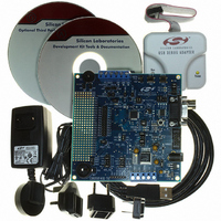
KIT DEV FOR C8051F41X
Manufacturer
Silicon Laboratories Inc
Type
MCUr
Specifications of C8051F410DK
Contents
Evaluation Board, Power Supply, USB Cables, Adapter and Documentation
Processor To Be Evaluated
C8051F41x
Interface Type
USB
Silicon Manufacturer
Silicon Labs
Core Architecture
8051
Silicon Core Number
C8051F410
Silicon Family Name
C8051F41x
Lead Free Status / RoHS Status
Contains lead / RoHS non-compliant
For Use With/related Products
Silicon Laboratories C8051F41x
Lead Free Status / Rohs Status
Lead free / RoHS Compliant
Other names
336-1314
Available stocks
Company
Part Number
Manufacturer
Quantity
Price
Company:

Part Number:
C8051F410DK
Manufacturer:
Silicon Labs
Quantity:
135


C8051F410/1/2/3
16.4.2. 16.4.2 PSWE Maintenance
16.4.3. System Clock
140
7. Reduce the number of places in code where the PSWE bit (b0 in PSCTL) is set to a '1'. There
8. Minimize the number of variable accesses while PSWE is set to a '1'. Handle pointer address
9. Disable interrupts prior to setting PSWE to a '1' and leave them disabled until after PSWE has
10. Make certain that the Flash write and erase pointer variables are not located in XRAM. See
11. Add address bounds checking to the routines that write or erase Flash memory to ensure that
12. If operating from an external crystal, be advised that crystal performance is susceptible to
13. If operating from the external oscillator, switch to the internal oscillator during Flash write or
should be exactly one routine in code that sets PSWE to a '1' to write Flash bytes and one rou-
tine in code that sets both PSWE and PSEE both to a '1' to erase Flash pages.
updates and loop maintenance outside the "PSWE = 1; ... PSWE = 0;" area. Code examples
showing this can be found in AN201, "Writing to Flash from Firmware", available from the Sili-
con Laboratories web site.
been reset to '0'. Any interrupts posted during the Flash write or erase operation will be ser-
viced in priority order after the Flash operation has been completed and interrupts have been
re-enabled by software.
your compiler documentation for instructions regarding how to explicitly locate variables in dif-
ferent memory areas.
a routine called with an illegal address does not result in modification of the Flash.
electrical interference and is sensitive to layout and to changes in temperature. If the system is
operating in an electrically noisy environment, use the internal oscillator or use an external
CMOS clock.
erase operations. The external oscillator can continue to run, and the CPU can switch back to
the external oscillator after the Flash operation has completed.
Rev. 1.1
Related parts for C8051F410DK
Image
Part Number
Description
Manufacturer
Datasheet
Request
R

Part Number:
Description:
SMD/C°/SINGLE-ENDED OUTPUT SILICON OSCILLATOR
Manufacturer:
Silicon Laboratories Inc
Part Number:
Description:
Manufacturer:
Silicon Laboratories Inc
Datasheet:
Part Number:
Description:
N/A N/A/SI4010 AES KEYFOB DEMO WITH LCD RX
Manufacturer:
Silicon Laboratories Inc
Datasheet:
Part Number:
Description:
N/A N/A/SI4010 SIMPLIFIED KEY FOB DEMO WITH LED RX
Manufacturer:
Silicon Laboratories Inc
Datasheet:
Part Number:
Description:
N/A/-40 TO 85 OC/EZLINK MODULE; F930/4432 HIGH BAND (REV E/B1)
Manufacturer:
Silicon Laboratories Inc
Part Number:
Description:
EZLink Module; F930/4432 Low Band (rev e/B1)
Manufacturer:
Silicon Laboratories Inc
Part Number:
Description:
I°/4460 10 DBM RADIO TEST CARD 434 MHZ
Manufacturer:
Silicon Laboratories Inc
Part Number:
Description:
I°/4461 14 DBM RADIO TEST CARD 868 MHZ
Manufacturer:
Silicon Laboratories Inc
Part Number:
Description:
I°/4463 20 DBM RFSWITCH RADIO TEST CARD 460 MHZ
Manufacturer:
Silicon Laboratories Inc
Part Number:
Description:
I°/4463 20 DBM RADIO TEST CARD 868 MHZ
Manufacturer:
Silicon Laboratories Inc
Part Number:
Description:
I°/4463 27 DBM RADIO TEST CARD 868 MHZ
Manufacturer:
Silicon Laboratories Inc
Part Number:
Description:
I°/4463 SKYWORKS 30 DBM RADIO TEST CARD 915 MHZ
Manufacturer:
Silicon Laboratories Inc
Part Number:
Description:
N/A N/A/-40 TO 85 OC/4463 RFMD 30 DBM RADIO TEST CARD 915 MHZ
Manufacturer:
Silicon Laboratories Inc
Part Number:
Description:
I°/4463 20 DBM RADIO TEST CARD 169 MHZ
Manufacturer:
Silicon Laboratories Inc