C8051F410DK Silicon Laboratories Inc, C8051F410DK Datasheet - Page 63
C8051F410DK
Manufacturer Part Number
C8051F410DK
Description
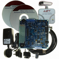
KIT DEV FOR C8051F41X
Manufacturer
Silicon Laboratories Inc
Type
MCUr
Specifications of C8051F410DK
Contents
Evaluation Board, Power Supply, USB Cables, Adapter and Documentation
Processor To Be Evaluated
C8051F41x
Interface Type
USB
Silicon Manufacturer
Silicon Labs
Core Architecture
8051
Silicon Core Number
C8051F410
Silicon Family Name
C8051F41x
Lead Free Status / RoHS Status
Contains lead / RoHS non-compliant
For Use With/related Products
Silicon Laboratories C8051F41x
Lead Free Status / Rohs Status
Lead free / RoHS Compliant
Other names
336-1314
Available stocks
Company
Part Number
Manufacturer
Quantity
Price
Company:

Part Number:
C8051F410DK
Manufacturer:
Silicon Labs
Quantity:
135


5.4.
The ADC Programmable Window Detector continuously compares the ADC0 output registers to user-pro-
grammed limits, and notifies the system when a desired condition is detected. This is especially effective in
an interrupt-driven system, saving code space and CPU bandwidth while delivering faster system
response times. The window detector interrupt flag (AD0WINT in register ADC0CN) can also be used in
polled mode. The ADC0 Greater-Than (ADC0GTH, ADC0GTL) and Less-Than (ADC0LTH, ADC0LTL)
registers hold the comparison values. The window detector flag can be programmed to indicate when mea-
sured data is inside or outside of the user-programmed limits, depending on the contents of the ADC0
Less-Than and ADC0 Greater-Than registers.
Bits7–4: AD0PWR3–0: ADC0 Burst Power-Up Time.
Bits3–2: AD0TM1–0: ADC0 Tracking Mode Select Bits.
Bits1–0: AD0TK1–0: ADC0 Post-Track Time.
R/W
Bit7
Programmable Window Detector
For BURSTEN = 0:
ADC0 power state controlled by AD0EN.
For BURSTEN = 1 and AD0EN = 1;
ADC0 remains enabled and does not enter the low power state.
For BURSTEN = 1 and AD0EN = 0:
ADC0 enters the low power state as specified in Table 5.3 and Table 5.4 and is enabled
after each convert start signal. The Power Up time is programmed according to the following
equation:
00: Reserved.
01: ADC0 is configured to Post-Tracking Mode.
10: ADC0 is configured to Pre-Tracking Mode.
11: ADC0 is configured to Dual-Tracking Mode (default).
Post-Tracking time is controlled by AD0TK as follows:
00: Post-Tracking time is equal to 2 SAR clock cycles + 2 FCLK cycles.
01: Post-Tracking time is equal to 4 SAR clock cycles + 2 FCLK cycles.
10: Post-Tracking time is equal to 8 SAR clock cycles + 2 FCLK cycles.
11: Post-Tracking time is equal to 16 SAR clock cycles + 2 FCLK cycles.
AD0PWR
SFR Definition 5.6. ADC0TK: ADC0 Tracking Mode Select
R/W
Bit6
AD0PWR
=
Tstartup
---------------------- 1
R/W
Bit5
400ns
–
R/W
Bit4
or
Tstartup
Rev. 1.1
R/W
Bit3
AD0TM
=
R/W
Bit2
AD0PWR
C8051F410/1/2/3
R/W
Bit1
+
AD0TK
1
(bit addressable)
400ns
R/W
Bit0
SFR Address:
Reset Value
11111111
0xBA
63
Related parts for C8051F410DK
Image
Part Number
Description
Manufacturer
Datasheet
Request
R

Part Number:
Description:
SMD/C°/SINGLE-ENDED OUTPUT SILICON OSCILLATOR
Manufacturer:
Silicon Laboratories Inc
Part Number:
Description:
Manufacturer:
Silicon Laboratories Inc
Datasheet:
Part Number:
Description:
N/A N/A/SI4010 AES KEYFOB DEMO WITH LCD RX
Manufacturer:
Silicon Laboratories Inc
Datasheet:
Part Number:
Description:
N/A N/A/SI4010 SIMPLIFIED KEY FOB DEMO WITH LED RX
Manufacturer:
Silicon Laboratories Inc
Datasheet:
Part Number:
Description:
N/A/-40 TO 85 OC/EZLINK MODULE; F930/4432 HIGH BAND (REV E/B1)
Manufacturer:
Silicon Laboratories Inc
Part Number:
Description:
EZLink Module; F930/4432 Low Band (rev e/B1)
Manufacturer:
Silicon Laboratories Inc
Part Number:
Description:
I°/4460 10 DBM RADIO TEST CARD 434 MHZ
Manufacturer:
Silicon Laboratories Inc
Part Number:
Description:
I°/4461 14 DBM RADIO TEST CARD 868 MHZ
Manufacturer:
Silicon Laboratories Inc
Part Number:
Description:
I°/4463 20 DBM RFSWITCH RADIO TEST CARD 460 MHZ
Manufacturer:
Silicon Laboratories Inc
Part Number:
Description:
I°/4463 20 DBM RADIO TEST CARD 868 MHZ
Manufacturer:
Silicon Laboratories Inc
Part Number:
Description:
I°/4463 27 DBM RADIO TEST CARD 868 MHZ
Manufacturer:
Silicon Laboratories Inc
Part Number:
Description:
I°/4463 SKYWORKS 30 DBM RADIO TEST CARD 915 MHZ
Manufacturer:
Silicon Laboratories Inc
Part Number:
Description:
N/A N/A/-40 TO 85 OC/4463 RFMD 30 DBM RADIO TEST CARD 915 MHZ
Manufacturer:
Silicon Laboratories Inc
Part Number:
Description:
I°/4463 20 DBM RADIO TEST CARD 169 MHZ
Manufacturer:
Silicon Laboratories Inc