C8051F410DK Silicon Laboratories Inc, C8051F410DK Datasheet - Page 82
C8051F410DK
Manufacturer Part Number
C8051F410DK
Description
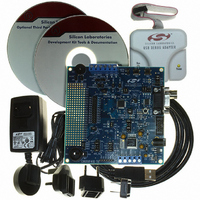
KIT DEV FOR C8051F41X
Manufacturer
Silicon Laboratories Inc
Type
MCUr
Specifications of C8051F410DK
Contents
Evaluation Board, Power Supply, USB Cables, Adapter and Documentation
Processor To Be Evaluated
C8051F41x
Interface Type
USB
Silicon Manufacturer
Silicon Labs
Core Architecture
8051
Silicon Core Number
C8051F410
Silicon Family Name
C8051F41x
Lead Free Status / RoHS Status
Contains lead / RoHS non-compliant
For Use With/related Products
Silicon Laboratories C8051F41x
Lead Free Status / Rohs Status
Lead free / RoHS Compliant
Other names
336-1314
Available stocks
Company
Part Number
Manufacturer
Quantity
Price
Company:

Part Number:
C8051F410DK
Manufacturer:
Silicon Labs
Quantity:
135


C8051F410/1/2/3
Table 8.1. Voltage Regulator Electrical Specifications
V
82
Input Voltage Range (V
Load Current
Load Regulation
Output Voltage (V
Bias Current
Dropout Indicator Detection
Threshold
Output Voltage Tempco
VREG Settling Time
*Note: Actual Output Voltage (V
DD
Bit 7:
Bit 6:
Bit 5:
Bit 4:
Bits 3–1: UNUSED. Read = 0b. Write = don’t care.
Bit 0:
REGDIS Reserved
= 2.1 or 2.5 V; –40 to +85 °C unless otherwise specified. Typical values are given at 25 ºC.
R/W
Bit7
Parameter
REGDIS: Voltage Regulator Disable Bit.
This bit disables/enables the Voltage Regulator.
0: Voltage Regulator Enabled.
1: Voltage Regulator Disabled.
RESERVED. Read = 0b. Must write 0b.
UNUSED. Read = 0b. Write = don’t care.
REG0MD: Voltage Regulator Mode Select Bit.
This bit selects the Voltage Regulator output voltage.
0: Voltage Regulator output is 2.1 V.
1: Voltage Regulator output is 2.5 V (default).
DROPOUT: Voltage Regulator Dropout Indicator Bit.
0: Voltage Regulator is not in dropout.
1: Voltage Regulator is in or near dropout.
R/W
Bit6
DD
)
SFR Definition 8.1. REG0CN: Regulator Control
REGIN
Bit5
—
)*
R
DD
) = Nominal Output Voltage (V
Output Current = 1 mA
REG0MD = ‘0’
REG0MD = ‘1’
REG0MD = ‘0’
REG0MD = ‘1’
50 mA load with V
and V
REG0MD
DD
R/W
Bit4
load capacitor of 4.8 µF
Conditions
Rev. 1.1
REGIN
Bit3
—
R
= 2.5 V
DD
) – (Load Regulation x Load Current).
Bit2
—
R
(See Note)
2.35
Min
2.0
—
—
—
—
—
—
—
Bit1
—
R
DROPOUT 00010000
Typ
600
250
SFR Address:
2.1
2.5
65
—
—
7
1
1
Bit0
R
Max
5.25
2.25
2.55
1.5
1.5
50
15
—
—
—
0xC9
Reset Value
mV/mA
µV/ºC
Units
mA
mV
µA
µs
V
V
Related parts for C8051F410DK
Image
Part Number
Description
Manufacturer
Datasheet
Request
R

Part Number:
Description:
SMD/C°/SINGLE-ENDED OUTPUT SILICON OSCILLATOR
Manufacturer:
Silicon Laboratories Inc
Part Number:
Description:
Manufacturer:
Silicon Laboratories Inc
Datasheet:
Part Number:
Description:
N/A N/A/SI4010 AES KEYFOB DEMO WITH LCD RX
Manufacturer:
Silicon Laboratories Inc
Datasheet:
Part Number:
Description:
N/A N/A/SI4010 SIMPLIFIED KEY FOB DEMO WITH LED RX
Manufacturer:
Silicon Laboratories Inc
Datasheet:
Part Number:
Description:
N/A/-40 TO 85 OC/EZLINK MODULE; F930/4432 HIGH BAND (REV E/B1)
Manufacturer:
Silicon Laboratories Inc
Part Number:
Description:
EZLink Module; F930/4432 Low Band (rev e/B1)
Manufacturer:
Silicon Laboratories Inc
Part Number:
Description:
I°/4460 10 DBM RADIO TEST CARD 434 MHZ
Manufacturer:
Silicon Laboratories Inc
Part Number:
Description:
I°/4461 14 DBM RADIO TEST CARD 868 MHZ
Manufacturer:
Silicon Laboratories Inc
Part Number:
Description:
I°/4463 20 DBM RFSWITCH RADIO TEST CARD 460 MHZ
Manufacturer:
Silicon Laboratories Inc
Part Number:
Description:
I°/4463 20 DBM RADIO TEST CARD 868 MHZ
Manufacturer:
Silicon Laboratories Inc
Part Number:
Description:
I°/4463 27 DBM RADIO TEST CARD 868 MHZ
Manufacturer:
Silicon Laboratories Inc
Part Number:
Description:
I°/4463 SKYWORKS 30 DBM RADIO TEST CARD 915 MHZ
Manufacturer:
Silicon Laboratories Inc
Part Number:
Description:
N/A N/A/-40 TO 85 OC/4463 RFMD 30 DBM RADIO TEST CARD 915 MHZ
Manufacturer:
Silicon Laboratories Inc
Part Number:
Description:
I°/4463 20 DBM RADIO TEST CARD 169 MHZ
Manufacturer:
Silicon Laboratories Inc