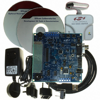
C8051F410DK Silicon Laboratories Inc, C8051F410DK Datasheet - Page 141

C8051F410DK
Manufacturer Part Number
C8051F410DK
Description
KIT DEV FOR C8051F41X
Manufacturer
Silicon Laboratories Inc
Type
MCUr
Specifications of C8051F410DK
Contents
Evaluation Board, Power Supply, USB Cables, Adapter and Documentation
Processor To Be Evaluated
C8051F41x
Interface Type
USB
Silicon Manufacturer
Silicon Labs
Core Architecture
8051
Silicon Core Number
C8051F410
Silicon Family Name
C8051F41x
Lead Free Status / RoHS Status
Contains lead / RoHS non-compliant
For Use With/related Products
Silicon Laboratories C8051F41x
Lead Free Status / Rohs Status
Lead free / RoHS Compliant
Other names
336-1314
Available stocks
Company
Part Number
Manufacturer
Quantity
Price
Company:
Part Number:
C8051F410DK
Manufacturer:
Silicon Labs
Quantity:
135
- Current page: 141 of 270
- Download datasheet (2Mb)
Bits7–2: UNUSED: Read = 000000b, Write = don’t care.
Bit1:
Bit0:
Bits7–0: FLKEY: Flash Lock and Key Register
R/W
Bit7
Bit7
R
-
PSEE: Program Store Erase Enable
Setting this bit (in combination with PSWE) allows an entire page of Flash program memory
to be erased. If this bit is logic 1 and Flash writes are enabled (PSWE is logic 1), a write to
Flash memory using the MOVX instruction will erase the entire page that contains the loca-
tion addressed by the MOVX instruction. The value of the data byte written does not matter.
0: Flash program memory erasure disabled.
1: Flash program memory erasure enabled.
PSWE: Program Store Write Enable
Setting this bit allows writing a byte of data to the Flash program memory using the MOVX
write instruction. The Flash location should be erased before writing data.
0: Writes to Flash program memory disabled.
1: Writes to Flash program memory enabled; the MOVX write instruction targets Flash
memory.
Write:
This register provides a lock and key function for Flash erasures and writes. Flash writes
and erases are enabled by writing 0xA5 followed by 0xF1 to the FLKEY register. Flash
writes and erases are automatically disabled after the next write or erase is complete. If any
writes to FLKEY are performed incorrectly, or if a Flash write or erase operation is attempted
while these operations are disabled, the Flash will be permanently locked from writes or era-
sures until the next device reset. If an application never writes to Flash, it can intentionally
lock the Flash by writing a non-0xA5 value to FLKEY from software.
Read:
When read, bits 1-0 indicate the current Flash lock state.
00: Flash is write/erase locked.
01: The first key code has been written (0xA5).
10: Flash is unlocked (writes/erases allowed).
11: Flash writes/erases disabled until the next reset.
SFR Definition 16.1. PSCTL: Program Store R/W Control
R/W
Bit6
Bit6
R
-
SFR Definition 16.2. FLKEY: Flash Lock and Key
R/W
Bit5
Bit5
R
-
R/W
Bit4
Bit4
R
-
Rev. 1.1
R/W
Bit3
Bit3
R
-
R/W
Bit2
Bit2
R
-
C8051F410/1/2/3
PSEE
R/W
R/W
Bit1
Bit1
SFR Address:
SFR Address:
PSWE
R/W
R/W
Bit0
Bit0
0x8F
0xB7
00000000
Reset Value
00000000
Reset Value
141
Related parts for C8051F410DK
Image
Part Number
Description
Manufacturer
Datasheet
Request
R
Part Number:
Description:
SMD/C°/SINGLE-ENDED OUTPUT SILICON OSCILLATOR
Manufacturer:
Silicon Laboratories Inc
Part Number:
Description:
Manufacturer:
Silicon Laboratories Inc
Datasheet:
Part Number:
Description:
N/A N/A/SI4010 AES KEYFOB DEMO WITH LCD RX
Manufacturer:
Silicon Laboratories Inc
Datasheet:
Part Number:
Description:
N/A N/A/SI4010 SIMPLIFIED KEY FOB DEMO WITH LED RX
Manufacturer:
Silicon Laboratories Inc
Datasheet:
Part Number:
Description:
N/A/-40 TO 85 OC/EZLINK MODULE; F930/4432 HIGH BAND (REV E/B1)
Manufacturer:
Silicon Laboratories Inc
Part Number:
Description:
EZLink Module; F930/4432 Low Band (rev e/B1)
Manufacturer:
Silicon Laboratories Inc
Part Number:
Description:
I°/4460 10 DBM RADIO TEST CARD 434 MHZ
Manufacturer:
Silicon Laboratories Inc
Part Number:
Description:
I°/4461 14 DBM RADIO TEST CARD 868 MHZ
Manufacturer:
Silicon Laboratories Inc
Part Number:
Description:
I°/4463 20 DBM RFSWITCH RADIO TEST CARD 460 MHZ
Manufacturer:
Silicon Laboratories Inc
Part Number:
Description:
I°/4463 20 DBM RADIO TEST CARD 868 MHZ
Manufacturer:
Silicon Laboratories Inc
Part Number:
Description:
I°/4463 27 DBM RADIO TEST CARD 868 MHZ
Manufacturer:
Silicon Laboratories Inc
Part Number:
Description:
I°/4463 SKYWORKS 30 DBM RADIO TEST CARD 915 MHZ
Manufacturer:
Silicon Laboratories Inc
Part Number:
Description:
N/A N/A/-40 TO 85 OC/4463 RFMD 30 DBM RADIO TEST CARD 915 MHZ
Manufacturer:
Silicon Laboratories Inc
Part Number:
Description:
I°/4463 20 DBM RADIO TEST CARD 169 MHZ
Manufacturer:
Silicon Laboratories Inc


