C8051F410DK Silicon Laboratories Inc, C8051F410DK Datasheet - Page 51
C8051F410DK
Manufacturer Part Number
C8051F410DK
Description
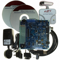
KIT DEV FOR C8051F41X
Manufacturer
Silicon Laboratories Inc
Type
MCUr
Specifications of C8051F410DK
Contents
Evaluation Board, Power Supply, USB Cables, Adapter and Documentation
Processor To Be Evaluated
C8051F41x
Interface Type
USB
Silicon Manufacturer
Silicon Labs
Core Architecture
8051
Silicon Core Number
C8051F410
Silicon Family Name
C8051F41x
Lead Free Status / RoHS Status
Contains lead / RoHS non-compliant
For Use With/related Products
Silicon Laboratories C8051F41x
Lead Free Status / Rohs Status
Lead free / RoHS Compliant
Other names
336-1314
Available stocks
Company
Part Number
Manufacturer
Quantity
Price
Company:

Part Number:
C8051F410DK
Manufacturer:
Silicon Labs
Quantity:
135


5.
The ADC0 subsystem for the C8051F41x consists of an analog multiplexer (AMUX0) with 27 total input
selections, and a 200 ksps, 12-bit successive-approximation-register ADC with integrated track-and-hold,
programmable window detector, and hardware accumulator. The ADC0 subsystem has a special Burst
Mode which can automatically enable ADC0, capture and accumulate samples, then place ADC0 in a low
power shutdown mode without CPU intervention. The AMUX0, data conversion modes, and window detec-
tor are all configurable under software control via the Special Function Registers shown in Figure 5.1.
ADC0 inputs are single-ended and may be configured to measure P0.0-P2.7, the Temperature Sensor out-
put, V
(ADC0CN) is set to logic 1, or when performing conversions in Burst Mode. ADC0 is in low power shut-
down when AD0EN is logic 0 and no Burst Mode conversions are taking place.
5.1.
AMUX0 selects the input channel to the ADC. Any of the following may be selected as an input: P0.0-P2.7,
the on-chip temperature sensor, the core power supply (V
and all signals measured are with respect to GND. The ADC0 input channels are selected using the
ADC0MX register as described in SFR Definition 5.1.
Important Note About ADC0 Input Configuration: Port pins selected as ADC0 inputs should be config-
ured as analog inputs and should be skipped by the Digital Crossbar. To configure a Port pin for analog
input, set to ‘0’ the corresponding bit in register PnMDIN (for n = 0,1,2) and write a ‘1’ in the corresponding
Port Latch register Pn (for n = 0,1,2). To force the Crossbar to skip a Port pin, set to ‘1’ the corresponding
bit in register PnSKIP (for n = 0,1,2). See
configuration details.
DD
12-Bit ADC (ADC0)
Analog Multiplexer
, or GND with respect to GND. ADC0 is enabled when the AD0EN bit in the ADC0 Control register
P0.0
P0.7
P1.0
P1.7
P2.0
P2.7
Temp Sensor
VDD
GND
27-to-1
AMUX
Figure 5.1. ADC0 Functional Block Diagram
ADC0MX
P2.3-P2.6 available on
‘F410/2
25 MHz Max
Burst Mode
Oscillator
Conversion
SYSCLK
Section “18. Port Input/Output” on page 147
Start
Rev. 1.1
Burst Mode
ADC0TK
Logic
ADC0CF
DD
ADC
12-Bit
SAR
), or ground (GND). ADC0 is single-ended
ADC0GTH ADC0GTL
ADC0LTH
VDD
ADC0CN
C8051F410/1/2/3
ADC0LTL
Conversion
Start
00
01
10
11
32
for more Port I/O
Accumulator
AD0WINT
Compare
Window
AD0BUSY (W)
Timer 3 Overflow
CNVSTR Input
Timer 2 Overflow
Logic
51
Related parts for C8051F410DK
Image
Part Number
Description
Manufacturer
Datasheet
Request
R

Part Number:
Description:
SMD/C°/SINGLE-ENDED OUTPUT SILICON OSCILLATOR
Manufacturer:
Silicon Laboratories Inc
Part Number:
Description:
Manufacturer:
Silicon Laboratories Inc
Datasheet:
Part Number:
Description:
N/A N/A/SI4010 AES KEYFOB DEMO WITH LCD RX
Manufacturer:
Silicon Laboratories Inc
Datasheet:
Part Number:
Description:
N/A N/A/SI4010 SIMPLIFIED KEY FOB DEMO WITH LED RX
Manufacturer:
Silicon Laboratories Inc
Datasheet:
Part Number:
Description:
N/A/-40 TO 85 OC/EZLINK MODULE; F930/4432 HIGH BAND (REV E/B1)
Manufacturer:
Silicon Laboratories Inc
Part Number:
Description:
EZLink Module; F930/4432 Low Band (rev e/B1)
Manufacturer:
Silicon Laboratories Inc
Part Number:
Description:
I°/4460 10 DBM RADIO TEST CARD 434 MHZ
Manufacturer:
Silicon Laboratories Inc
Part Number:
Description:
I°/4461 14 DBM RADIO TEST CARD 868 MHZ
Manufacturer:
Silicon Laboratories Inc
Part Number:
Description:
I°/4463 20 DBM RFSWITCH RADIO TEST CARD 460 MHZ
Manufacturer:
Silicon Laboratories Inc
Part Number:
Description:
I°/4463 20 DBM RADIO TEST CARD 868 MHZ
Manufacturer:
Silicon Laboratories Inc
Part Number:
Description:
I°/4463 27 DBM RADIO TEST CARD 868 MHZ
Manufacturer:
Silicon Laboratories Inc
Part Number:
Description:
I°/4463 SKYWORKS 30 DBM RADIO TEST CARD 915 MHZ
Manufacturer:
Silicon Laboratories Inc
Part Number:
Description:
N/A N/A/-40 TO 85 OC/4463 RFMD 30 DBM RADIO TEST CARD 915 MHZ
Manufacturer:
Silicon Laboratories Inc
Part Number:
Description:
I°/4463 20 DBM RADIO TEST CARD 169 MHZ
Manufacturer:
Silicon Laboratories Inc