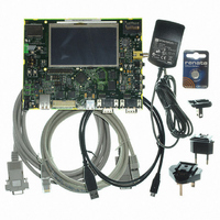
AT91SAM9G45-EKES Atmel, AT91SAM9G45-EKES Datasheet - Page 25

AT91SAM9G45-EKES
Manufacturer Part Number
AT91SAM9G45-EKES
Description
KIT EVAL FOR AT91SAM9G45
Manufacturer
Atmel
Series
AT91SAM Smart ARMr
Type
MCUr
Datasheets
1.AT91SAM9G45-EKES.pdf
(56 pages)
2.AT91SAM9G45-EKES.pdf
(1218 pages)
3.AT91SAM9G45-EKES.pdf
(66 pages)
Specifications of AT91SAM9G45-EKES
Contents
Board
Processor To Be Evaluated
SAM9G45
Data Bus Width
32 bit
Interface Type
I2C, SPI, UART
Maximum Operating Temperature
+ 50 C
Minimum Operating Temperature
- 10 C
Operating Supply Voltage
1.8 V to 3.3 V
For Use With/related Products
AT91SAM9G45
Lead Free Status / RoHS Status
Lead free / RoHS Compliant
Other names
Q4626953
7.2.2
Table 7-1.
7.2.3
7.2.4
6438ES–ATARM–21-Jun-10
seen at 0x100000 through AHB
SRAM A ITCM size (KBytes)
TCM Interface
Internal ROM
Boot Strategies
ITCM and DTCM Memory Configuration
32
0
0
On the processor side, this Internal SRAM can be allocated to two areas.
Within the 64 Kbyte SRAM size available, the amount of memory assigned to each block is soft-
ware programmable according to
The AT91SAM9G45 embeds an Internal ROM, which contains the bootrom and SAM-BA
program.
At any time, the ROM is mapped at address 0x0040 0000. It is also accessible at address 0x0
(BMS =1) after the reset and before the Remap Command.
The system always boots at address 0x0. To ensure maximum boot possibilities the memory
layout can be changed with two parameters.
REMAP allows the user to layout the internal SRAM bank to 0x0 to ease the development. This
is done by software once the system has boot.
BMS allows the user to lay out to 0x0, when convenient, the ROM or an external memory. This is
done by a hardware way at reset.
Note: All the memory blocks can always be seen at their specified base addresses that are not
concerned by these parameters.
The AT91SAM9G45 Bus Matrix manages a boot memory that depends on the level on the pin
BMS at reset. The internal memory area mapped between address 0x0 and 0x000F FFFF is
reserved to this effect.
• Internal SRAM A is the ARM926EJ-S Instruction TCM. The user can map this SRAM block
• Internal SRAM B is the ARM926EJ-S Data TCM. The user can map this SRAM block
• Internal SRAM C is only accessible by all the AHB Masters. After reset and until the Remap
anywhere in the ARM926 instruction memory space using CP15 instructions and the TCR
configuration register located in the Chip Configuration User Interface. This SRAM block is
also accessible by the ARM926 Masters and by the AHB Masters through the AHB bus
anywhere in the ARM926 data memory space using CP15 instructions. This SRAM block is
also accessible by the ARM926 Data Master and by the AHB Masters through the AHB bus.
Command is performed, this SRAM block is accessible through the AHB bus at address
0x0030 0000 by all the AHB Masters. After Remap, this SRAM block also becomes
accessible through the AHB bus at address 0x0 by the ARM926 Instruction and the ARM926
Data Masters.
seen at 0x200000 through AHB
SRAM B DTCM size (KBytes)
64
32
0
Table
7-1.
seen at 0x300000 through AHB
SRAM C (KBytes)
64
0
0
AT91SAM9G45
25


