MC56F8323EVM Freescale Semiconductor, MC56F8323EVM Datasheet - Page 93
MC56F8323EVM
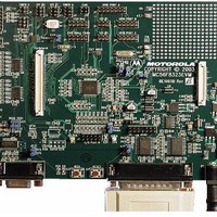
Manufacturer Part Number
MC56F8323EVM
Description
KIT EVALUATION FOR MC56F8323
Manufacturer
Freescale Semiconductor
Type
DSPr
Datasheets
1.CWH-UTP-ONCE-HE.pdf
(2 pages)
2.MC56F8323EVM.pdf
(72 pages)
3.MC56F8323EVME.pdf
(140 pages)
Specifications of MC56F8323EVM
Contents
Module and Misc Hardware
Processor To Be Evaluated
MC56F8322 and MC56F8323
Data Bus Width
16 bit
Interface Type
RS-232
For Use With/related Products
MC56F8322, MC56F8323
Lead Free Status / RoHS Status
Contains lead / RoHS non-compliant


6.5.8.5
This bit selects the alternate function for GPIOB0.
6.5.8.6
This bit selects the alternate function for GPIOA5.
6.5.8.7
This bit selects the alternate function for GPIOA4.
6.5.8.8
This bit selects the alternate function for GPIOA3.
6.5.8.9
This bit selects the alternate function for GPIOA2.
6.5.9
The Peripheral Clock Enable register is used to enable or disable clocks to the peripherals as a power
savings feature. The clocks can be individually controlled for each peripheral on the chip.
6.5.9.1
This bit field is reserved or not implemented. It is read as 1 and cannot be modified by writing.
Freescale Semiconductor
Preliminary
•
•
•
•
•
•
•
•
•
•
Base + $C
RESET
Read
Write
0 = SS0 (default)
1 = TXD1
0 = PWMA5
1 = SCLK1
0 = PWMA4
1 = MOS1
0 = PWMA3
1 = MISO1
0 = PWMA2
1 = SS1
Peripheral Clock Enable Register (SIM_PCE)
GPIOB0 (B0)—Bit 4
GPIOA5 (A5)—Bit 3
GPIOA4 (A4)—Bit 2
GPIOA3 (A3)—Bit 1
GPIOA2 (A2)—Bit 0
Reserved—Bits 15–14
15
1
1
Figure 6-12 Peripheral Clock Enable Register (SIM_PCE)
14
1
1
ADCA
13
1
CAN
12
1
11
1
1
56F8323 Technical Data, Rev. 17
DEC0
10
1
9
1
1
TMRC
8
1
7
1
1
TMRA
6
1
SCI 1 SCI 0
5
1
4
1
SPI1
3
1
SPI0
2
1
Register Descriptions
1
1
1
PWMA
0
1
93
Related parts for MC56F8323EVM
Image
Part Number
Description
Manufacturer
Datasheet
Request
R

Part Number:
Description:
Manufacturer:
Freescale Semiconductor, Inc
Datasheet:
Part Number:
Description:
Manufacturer:
Freescale Semiconductor, Inc
Datasheet:
Part Number:
Description:
Manufacturer:
Freescale Semiconductor, Inc
Datasheet:
Part Number:
Description:
Manufacturer:
Freescale Semiconductor, Inc
Datasheet:
Part Number:
Description:
Manufacturer:
Freescale Semiconductor, Inc
Datasheet:
Part Number:
Description:
Manufacturer:
Freescale Semiconductor, Inc
Datasheet:
Part Number:
Description:
Manufacturer:
Freescale Semiconductor, Inc
Datasheet:
Part Number:
Description:
Manufacturer:
Freescale Semiconductor, Inc
Datasheet:
Part Number:
Description:
Manufacturer:
Freescale Semiconductor, Inc
Datasheet:
Part Number:
Description:
Manufacturer:
Freescale Semiconductor, Inc
Datasheet:
Part Number:
Description:
Manufacturer:
Freescale Semiconductor, Inc
Datasheet:
Part Number:
Description:
Manufacturer:
Freescale Semiconductor, Inc
Datasheet:
Part Number:
Description:
Manufacturer:
Freescale Semiconductor, Inc
Datasheet:
Part Number:
Description:
Manufacturer:
Freescale Semiconductor, Inc
Datasheet:
Part Number:
Description:
Manufacturer:
Freescale Semiconductor, Inc
Datasheet: