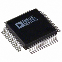
ADUC841BSZ62-5 Analog Devices Inc, ADUC841BSZ62-5 Datasheet - Page 10

ADUC841BSZ62-5
Manufacturer Part Number
ADUC841BSZ62-5
Description
IC ADC/DAC 12BIT W/MCU 52-MQFP
Manufacturer
Analog Devices Inc
Series
MicroConverter® ADuC8xxr
Datasheet
1.EVAL-ADUC842QS.pdf
(88 pages)
Specifications of ADUC841BSZ62-5
Core Size
8-Bit
Program Memory Size
62KB (62K x 8)
Core Processor
8052
Speed
20MHz
Connectivity
I²C, SPI, UART/USART
Peripherals
DMA, PSM, PWM, Temp Sensor, WDT
Number Of I /o
32
Program Memory Type
FLASH
Ram Size
2.25K x 8
Voltage - Supply (vcc/vdd)
4.75 V ~ 5.25 V
Data Converters
A/D 8x12b, D/A 2x12b
Oscillator Type
Internal
Operating Temperature
-40°C ~ 85°C
Package / Case
52-MQFP, 52-PQFP
Controller Family/series
(8051) 8052
No. Of I/o's
32
Ram Memory Size
2.25KB
Cpu Speed
20MIPS
No. Of Timers
3
No. Of Pwm Channels
2
Embedded Interface Type
UART
Rohs Compliant
Yes
Cpu Family
ADuC8xx
Device Core
8052
Device Core Size
8b
Frequency (max)
20MHz
Interface Type
I2C/SPI/UART
Total Internal Ram Size
2.25KB
# I/os (max)
34
Number Of Timers - General Purpose
3
Operating Supply Voltage (typ)
5V
Operating Supply Voltage (max)
5.25V
Operating Supply Voltage (min)
4.75V
On-chip Adc
8-chx12-bit
On-chip Dac
2-chx12-bit
Instruction Set Architecture
CISC
Operating Temp Range
-40C to 85C
Operating Temperature Classification
Industrial
Mounting
Surface Mount
Pin Count
52
Package Type
MQFP
Lead Free Status / RoHS Status
Lead free / RoHS Compliant
For Use With
EVAL-ADUC841QSZ - KIT DEV FOR ADUC841 QUICK START
Eeprom Size
-
Lead Free Status / Rohs Status
Compliant
Available stocks
Company
Part Number
Manufacturer
Quantity
Price
Company:
Part Number:
ADUC841BSZ62-5
Manufacturer:
Analog Devices Inc
Quantity:
135
Company:
Part Number:
ADUC841BSZ62-5
Manufacturer:
Analog Devices Inc
Quantity:
10 000
ADuC841/ADuC842/ADuC843
Mnemonic
P3.0–P3.7
PWMC
PWM0
PWM1
RxD
TxD
INT0
INT1
T0
T1
CONVST
EXTCLK
WR
RD
XTAL2
XTAL1
DGND
P2.0–P2.7
(A8–A15)
(A16–A23)
PSEN
ALE
EA
P0.7–P0.0
(A0-A7)
Types: P = Power, G = Ground, I= Input, O = Output., NC = No Connect
I/O
O
I
Type
I
O
O
I/O
O
I
I
I
I
I
I
O
O
G
I/O
O
O
I
I/O
Function
Port 3 is a bidirectional port with internal pull-up resistors. Port 3 pins that have 1s written to them are pulled high
by the internal pull-up resistors, and in that state can be used as inputs. As inputs, Port 3 pins being pulled
externally low source current because of the internal pull-up resistors. Port 3 pins also contain various secondary
functions, which are described below.
PWM Clock Input.
PWM0 Voltage Output. PWM outputs can be configured to use Ports 2.6 and 2.7 or Ports 3.4 and 3.3.
PWM1 Voltage Output. See the CFG841/CFG842 register for further information.
Receiver Data Input (Asynchronous) or Data Input/Output (Synchronous) of the Serial (UART) Port.
Transmitter Data Output (Asynchronous) or Clock Output (Synchronous) of the Serial (UART) Port.
Interrupt 0. Programmable edge or level triggered interrupt input; can be programmed to one of two priority
levels. This pin can also be used as a gate control input to Timer 0.
Interrupt 1. Programmable edge or level triggered interrupt input; can be programmed to one of two priority
levels. This pin can also be used as a gate control input to Timer 1.
Timer/Counter 0 Input.
Timer/Counter 1 Input.
Active Low Convert Start Logic Input for the ADC Block when the External Convert Start Function is Enabled. A
low-to-high transition on this input puts the track-and-hold into hold mode and starts the conversion.
Input for External Clock Signal. Has to be enabled via the CFG842 register.
Write Control Signal, Logic Output. Latches the data byte from Port 0 into the external data memory.
Read Control Signal, Logic Output. Enables the external data memory to Port 0.
Output of the Inverting Oscillator Amplifier.
Input to the Inverting Oscillator Amplifier.
Digital Ground. Ground reference point for the digital circuitry.
Port 2 is a bidirectional port with internal pull-up resistors. Port 2 pins that have 1s written to them are pulled high
by the internal pull-up resistors, and in that state can be used as inputs. As inputs, Port 2 pins being pulled
externally low source current because of the internal pull-up resistors. Port 2 emits the middle and high-order
address bytes during accesses to the external 24-bit external data memory space.
Program Store Enable, Logic Output. This pin remains low during internal program execution. PSEN is used to
enable serial download mode when pulled low through a resistor on power-up or reset. On reset this pin will
momentarily become an input and the status of the pin is sampled. If there is no pulldown resistor in place the pin
will go momentarilly high and then user code will execute. If a pull-down resistor is in place, the embedded serial
download/debug kernel will execute.
Address Latch Enable, Logic Output. This output is used to latch the low byte and page byte for 24-bit address
space accesses of the address into external data memory.
External Access Enable, Logic Input. When held high, this input enables the device to fetch code from internal
program memory locations. The parts do not support external code memory. This pin should not be left floating.
Port 0 is an 8-bit open-drain bidirectional I/O port. Port 0 pins that have 1s written to them float, and in that state
can be used as high impedance inputs. Port 0 is also the multiplexed low-order address and data bus during
accesses to external data memory. In this application, it uses strong internal pull-ups when emitting 1s.
Rev. 0 | Page 10 of 88


