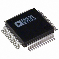
ADUC841BSZ62-5 Analog Devices Inc, ADUC841BSZ62-5 Datasheet - Page 45

ADUC841BSZ62-5
Manufacturer Part Number
ADUC841BSZ62-5
Description
IC ADC/DAC 12BIT W/MCU 52-MQFP
Manufacturer
Analog Devices Inc
Series
MicroConverter® ADuC8xxr
Datasheet
1.EVAL-ADUC842QS.pdf
(88 pages)
Specifications of ADUC841BSZ62-5
Core Size
8-Bit
Program Memory Size
62KB (62K x 8)
Core Processor
8052
Speed
20MHz
Connectivity
I²C, SPI, UART/USART
Peripherals
DMA, PSM, PWM, Temp Sensor, WDT
Number Of I /o
32
Program Memory Type
FLASH
Ram Size
2.25K x 8
Voltage - Supply (vcc/vdd)
4.75 V ~ 5.25 V
Data Converters
A/D 8x12b, D/A 2x12b
Oscillator Type
Internal
Operating Temperature
-40°C ~ 85°C
Package / Case
52-MQFP, 52-PQFP
Controller Family/series
(8051) 8052
No. Of I/o's
32
Ram Memory Size
2.25KB
Cpu Speed
20MIPS
No. Of Timers
3
No. Of Pwm Channels
2
Embedded Interface Type
UART
Rohs Compliant
Yes
Cpu Family
ADuC8xx
Device Core
8052
Device Core Size
8b
Frequency (max)
20MHz
Interface Type
I2C/SPI/UART
Total Internal Ram Size
2.25KB
# I/os (max)
34
Number Of Timers - General Purpose
3
Operating Supply Voltage (typ)
5V
Operating Supply Voltage (max)
5.25V
Operating Supply Voltage (min)
4.75V
On-chip Adc
8-chx12-bit
On-chip Dac
2-chx12-bit
Instruction Set Architecture
CISC
Operating Temp Range
-40C to 85C
Operating Temperature Classification
Industrial
Mounting
Surface Mount
Pin Count
52
Package Type
MQFP
Lead Free Status / RoHS Status
Lead free / RoHS Compliant
For Use With
EVAL-ADUC841QSZ - KIT DEV FOR ADUC841 QUICK START
Eeprom Size
-
Lead Free Status / Rohs Status
Compliant
Available stocks
Company
Part Number
Manufacturer
Quantity
Price
Company:
Part Number:
ADUC841BSZ62-5
Manufacturer:
Analog Devices Inc
Quantity:
135
Company:
Part Number:
ADUC841BSZ62-5
Manufacturer:
Analog Devices Inc
Quantity:
10 000
SERIAL PERIPHERAL INTERFACE (SPI)
The ADuC841/ADuC842/ADuC843 integrate a complete hard-
ware serial peripheral interface on-chip. SPI is an industry-
standard synchronous serial interface that allows 8 bits of data
to be synchronously transmitted and received simultaneously,
i.e., full duplex. Note that the SPI pins are shared with the I
pins. Therefore, the user can enable only one interface or the
other on these pins at any given time (see SPE in Table 18). SPI
can be operated at the same time as the I
MSPI bit in CFG841/CFG8842 is set. This moves the SPI
outputs (MISO, MOSI, and SCLOCK) to P3.3, P3.4, and P3.5,
respectively). The SPI port can be configured for master or slave
operation and typically consists of four pins, described in the
following sections.
MISO (Master In, Slave Out Data I/O Pin)
The MISO pin is configured as an input line in master mode
and as an output line in slave mode. The MISO line on the
master (data in) should be connected to the MISO line in the
slave device (data out). The data is transferred as byte-wide
(8-bit) serial data, MSB first.
MOSI (Master Out, Slave In Pin)
The MOSI pin is configured as an output line in master mode
and as an input line in slave mode. The MOSI line on the master
(data out) should be connected to the MOSI line in the slave
device (data in). The data is transferred as byte-wide (8-bit)
serial data, MSB first.
2
C interface if the
2
C
Rev. 0 | Page 45 of 88
SCLOCK (Serial Clock I/O Pin)
The master serial clock (SCLOCK) is used to synchronize the
data being transmitted and received through the MOSI and
MISO data lines. A single data bit is transmitted and received in
each SCLOCK period. Therefore, a byte is transmitted/received
after eight SCLOCK periods. The SCLOCK pin is configured as
an output in master mode and as an input in slave mode. In
master mode, the bit rate, polarity, and phase of the clock are
controlled by the CPOL, CPHA, SPR0, and SPR1 bits in the
SPICON SFR (see Table 18). In slave mode, the SPICON register
must be configured with the phase and polarity (CPHA and
CPOL) of the expected input clock. In both master and slave
modes, the data is transmitted on one edge of the SCLOCK
signal and sampled on the other. It is important, therefore, that
CPHA and CPOL are configured the same for the master and
slave devices.
SS (Slave Select Input Pin)
The SS pin is shared with the ADC5 input. To configure this pin
as a digital input, the bit must be cleared, e.g., CLR P1.5. This
line is active low. Data is received or transmitted in slave mode
only when the SS pin is low, allowing the parts to be used in
single-master, multislave SPI configurations. If CPHA = 1, the
SS input may be permanently pulled low. If CPHA = 0, the SS
input must be driven low before the first bit in a byte-wide
transmission or reception and return high again after the last bit
in that byte-wide transmission or reception. In SPI slave mode,
the logic level on the external SS pin can be read via the SPR0
bit in the SPICON SFR. The SFR registers, described in the
following tables, are used to control the SPI interface.
ADuC841/ADuC842/ADuC843


