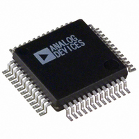
ADUC841BSZ62-5 Analog Devices Inc, ADUC841BSZ62-5 Datasheet - Page 40

ADUC841BSZ62-5
Manufacturer Part Number
ADUC841BSZ62-5
Description
IC ADC/DAC 12BIT W/MCU 52-MQFP
Manufacturer
Analog Devices Inc
Series
MicroConverter® ADuC8xxr
Datasheet
1.EVAL-ADUC842QS.pdf
(88 pages)
Specifications of ADUC841BSZ62-5
Core Size
8-Bit
Program Memory Size
62KB (62K x 8)
Core Processor
8052
Speed
20MHz
Connectivity
I²C, SPI, UART/USART
Peripherals
DMA, PSM, PWM, Temp Sensor, WDT
Number Of I /o
32
Program Memory Type
FLASH
Ram Size
2.25K x 8
Voltage - Supply (vcc/vdd)
4.75 V ~ 5.25 V
Data Converters
A/D 8x12b, D/A 2x12b
Oscillator Type
Internal
Operating Temperature
-40°C ~ 85°C
Package / Case
52-MQFP, 52-PQFP
Controller Family/series
(8051) 8052
No. Of I/o's
32
Ram Memory Size
2.25KB
Cpu Speed
20MIPS
No. Of Timers
3
No. Of Pwm Channels
2
Embedded Interface Type
UART
Rohs Compliant
Yes
Cpu Family
ADuC8xx
Device Core
8052
Device Core Size
8b
Frequency (max)
20MHz
Interface Type
I2C/SPI/UART
Total Internal Ram Size
2.25KB
# I/os (max)
34
Number Of Timers - General Purpose
3
Operating Supply Voltage (typ)
5V
Operating Supply Voltage (max)
5.25V
Operating Supply Voltage (min)
4.75V
On-chip Adc
8-chx12-bit
On-chip Dac
2-chx12-bit
Instruction Set Architecture
CISC
Operating Temp Range
-40C to 85C
Operating Temperature Classification
Industrial
Mounting
Surface Mount
Pin Count
52
Package Type
MQFP
Lead Free Status / RoHS Status
Lead free / RoHS Compliant
For Use With
EVAL-ADUC841QSZ - KIT DEV FOR ADUC841 QUICK START
Eeprom Size
-
Lead Free Status / Rohs Status
Compliant
Available stocks
Company
Part Number
Manufacturer
Quantity
Price
Company:
Part Number:
ADUC841BSZ62-5
Manufacturer:
Analog Devices Inc
Quantity:
135
Company:
Part Number:
ADUC841BSZ62-5
Manufacturer:
Analog Devices Inc
Quantity:
10 000
ADuC841/ADuC842/ADuC843
The endpoint nonlinearities illustrated in Figure 43 become
worse as a function of output loading. Most of the part’s
specifications assume a 10 kΩ resistive load to ground at the
DAC output. As the output is forced to source or sink more
current, the nonlinear regions at the top or bottom (respectively)
of Figure 43 become larger. Larger current demands can sig-
nificantly limit output voltage swing. Figure 44 and Figure 45
illustrate this behavior. Note that the upper trace in each of
these figures is valid only for an output range selection of
0 V-to-AV
high-side voltage drops as long as the reference voltage remains
below the upper trace in the corresponding figure. For example,
if AV
affected by loads less than 5 mA. But somewhere around 7 mA,
the upper curve in Figure 45 drops below 2.5 V (V
that at these higher currents the output is not capable of
reaching V
To reduce the effects of the saturation of the output amplifier at
values close to ground and to give reduced offset and gain errors,
the internal buffer can be bypassed. This is done by setting the
DBUF bit in the CFG841/CFG842 register. This allows a full
rail-to-rail output from the DAC, which should then be buffered
externally using a dual-supply op amp in order to get a rail-to-
rail output. This external buffer should be located as close as
physically possible to the DAC output pin on the PCB. Note that
the unbuffered mode works only in the 0 V to V
DD
= 3 V and V
DD
REF
. In 0 V-to-V
.
REF
= 2.5 V, the high-side voltage is not be
REF
mode, DAC loading does not cause
REF
REF
range.
), indicating
Rev. 0 | Page 40 of 88
To drive significant loads with the DAC outputs, external
buffering may be required (even with the internal buffer
enabled), as illustrated in Figure 46 . Table 11 lists some
recommended op amps.
The DAC output buffer also features a high impedance disable
function. In the chip’s default power-on state, both DACs are
disabled, and their outputs are in a high impedance state (or
three-state) where they remain inactive until enabled in
software. This means that if a zero output is desired during
power-up or power-down transient conditions, then a pull-
down resistor must be added to each DAC output. Assuming
this resistor is in place, the DAC outputs remain at ground
potential whenever the DAC is disabled.
Figure 46. Buffering the DAC Outputs
DAC0
DAC1
ADuC841/
ADuC842


