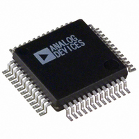
ADUC841BSZ62-5 Analog Devices Inc, ADUC841BSZ62-5 Datasheet - Page 72

ADUC841BSZ62-5
Manufacturer Part Number
ADUC841BSZ62-5
Description
IC ADC/DAC 12BIT W/MCU 52-MQFP
Manufacturer
Analog Devices Inc
Series
MicroConverter® ADuC8xxr
Datasheet
1.EVAL-ADUC842QS.pdf
(88 pages)
Specifications of ADUC841BSZ62-5
Core Size
8-Bit
Program Memory Size
62KB (62K x 8)
Core Processor
8052
Speed
20MHz
Connectivity
I²C, SPI, UART/USART
Peripherals
DMA, PSM, PWM, Temp Sensor, WDT
Number Of I /o
32
Program Memory Type
FLASH
Ram Size
2.25K x 8
Voltage - Supply (vcc/vdd)
4.75 V ~ 5.25 V
Data Converters
A/D 8x12b, D/A 2x12b
Oscillator Type
Internal
Operating Temperature
-40°C ~ 85°C
Package / Case
52-MQFP, 52-PQFP
Controller Family/series
(8051) 8052
No. Of I/o's
32
Ram Memory Size
2.25KB
Cpu Speed
20MIPS
No. Of Timers
3
No. Of Pwm Channels
2
Embedded Interface Type
UART
Rohs Compliant
Yes
Cpu Family
ADuC8xx
Device Core
8052
Device Core Size
8b
Frequency (max)
20MHz
Interface Type
I2C/SPI/UART
Total Internal Ram Size
2.25KB
# I/os (max)
34
Number Of Timers - General Purpose
3
Operating Supply Voltage (typ)
5V
Operating Supply Voltage (max)
5.25V
Operating Supply Voltage (min)
4.75V
On-chip Adc
8-chx12-bit
On-chip Dac
2-chx12-bit
Instruction Set Architecture
CISC
Operating Temp Range
-40C to 85C
Operating Temperature Classification
Industrial
Mounting
Surface Mount
Pin Count
52
Package Type
MQFP
Lead Free Status / RoHS Status
Lead free / RoHS Compliant
For Use With
EVAL-ADUC841QSZ - KIT DEV FOR ADUC841 QUICK START
Eeprom Size
-
Lead Free Status / Rohs Status
Compliant
Available stocks
Company
Part Number
Manufacturer
Quantity
Price
Company:
Part Number:
ADUC841BSZ62-5
Manufacturer:
Analog Devices Inc
Quantity:
135
Company:
Part Number:
ADUC841BSZ62-5
Manufacturer:
Analog Devices Inc
Quantity:
10 000
ADuC841/ADuC842/ADuC843
HARDWARE DESIGN CONSIDERATIONS
This section outlines some of the key hardware design
considerations that must be addressed when integrating the
ADuC841/ADuC842/ADuC843 into any hardware system.
Clock Oscillator
The clock source for the parts can be generated by the internal
PLL or by an external clock input. To use the internal PLL, con-
nect a 32.768 kHz parallel resonant crystal between XTAL1 and
XTAL2, and connect a capacitor from each pin to ground as
shown in Figure 75. The parts contain an internal capacitance of
18 pF on the XTAL1 and XTAL2 pins, which is sufficient for
most watch crystals. This crystal allows the PLL to lock correctly
to give an f
PLL will free run, giving an fVCO of 16.7 MHz ±20%. In this mode,
the CD bits are limited to CD = 1, giving a max core clock of
8.38 MHz. This is useful if an external clock input is required.
The part powers up and the PLL will free run; the user then
writes to the CFG842 SFR in software to enable the external clock
input on P3.4. Note that double the required clock must be pro-
vided externally since the part runs at CD = 1. A better solution is
to use the ADuC841 with the external clock.
For the ADuC841, connect the crystal in the same manner; external
capacitors should be connected as per the crystal manufacturer’s
recommendations. A minimum capacitance of 20 pF is
recommended on XTAL1 and XTAL2. The ADuC841 will not
operate if no crystal is present.
An external clock may be connected as shown in Figure 76 and
Figure 77.
EXTERNAL
SOURCE
Figure 76. Connecting an External Clock Source (ADuC841)
Figure 75. External Parallel Resonant Crystal Connections
CLOCK
VCO
of 16.777216 MHz. If no crystal is present, the
XTAL1
XTAL2
XTAL1
XTAL2
ADuC841
ADuC841/ADuC842/ADuC843
TO INTERNAL
TIMING CIRCUITS
TO INTERNAL
TIMING CIRCUITS
Rev. 0 | Page 72 of 88
Whether using the internal PLL or an external clock source, the
parts’ specified operational clock speed range is 400 kHz to
16.777216 MHz, (20 MHz, ADuC841). The core itself is static,
and functions all the way down to dc. But at clock speeds slower
that 400 kHz, the ADC can no longer function correctly. There-
fore, to ensure specified operation, use a clock frequency of at
least 400 kHz and no more than 20 MHz.
External Memory Interface
In addition to its internal program and data memories, the parts
can access up to 16 MBytes of external data memory (SRAM).
Note that the parts cannot access external program memory.
Figure 78 shows a hardware configuration for accessing up to
64 kBytes of external RAM. This interface is standard to any
8051 compatible MCU.
Figure 77. Connecting an External Clock Source (ADuC842/ADuC843)
Figure 78. External Data Memory Interface (64 kBytes Address Space)
ADuC841/
ADuC842/
ADuC843
EXTERNAL
SOURCE
CLOCK
ALE
WR
RD
P0
P2
P3.4
ADuC842/ADuC843
LATCH
TO INTERNAL
TIMING CIRCUITS
A0–A7
D0–D7
(DATA)
A8–A15
OE
WE
SRAM


