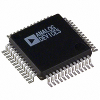
ADUC841BSZ62-5 Analog Devices Inc, ADUC841BSZ62-5 Datasheet - Page 24

ADUC841BSZ62-5
Manufacturer Part Number
ADUC841BSZ62-5
Description
IC ADC/DAC 12BIT W/MCU 52-MQFP
Manufacturer
Analog Devices Inc
Series
MicroConverter® ADuC8xxr
Datasheet
1.EVAL-ADUC842QS.pdf
(88 pages)
Specifications of ADUC841BSZ62-5
Core Size
8-Bit
Program Memory Size
62KB (62K x 8)
Core Processor
8052
Speed
20MHz
Connectivity
I²C, SPI, UART/USART
Peripherals
DMA, PSM, PWM, Temp Sensor, WDT
Number Of I /o
32
Program Memory Type
FLASH
Ram Size
2.25K x 8
Voltage - Supply (vcc/vdd)
4.75 V ~ 5.25 V
Data Converters
A/D 8x12b, D/A 2x12b
Oscillator Type
Internal
Operating Temperature
-40°C ~ 85°C
Package / Case
52-MQFP, 52-PQFP
Controller Family/series
(8051) 8052
No. Of I/o's
32
Ram Memory Size
2.25KB
Cpu Speed
20MIPS
No. Of Timers
3
No. Of Pwm Channels
2
Embedded Interface Type
UART
Rohs Compliant
Yes
Cpu Family
ADuC8xx
Device Core
8052
Device Core Size
8b
Frequency (max)
20MHz
Interface Type
I2C/SPI/UART
Total Internal Ram Size
2.25KB
# I/os (max)
34
Number Of Timers - General Purpose
3
Operating Supply Voltage (typ)
5V
Operating Supply Voltage (max)
5.25V
Operating Supply Voltage (min)
4.75V
On-chip Adc
8-chx12-bit
On-chip Dac
2-chx12-bit
Instruction Set Architecture
CISC
Operating Temp Range
-40C to 85C
Operating Temperature Classification
Industrial
Mounting
Surface Mount
Pin Count
52
Package Type
MQFP
Lead Free Status / RoHS Status
Lead free / RoHS Compliant
For Use With
EVAL-ADUC841QSZ - KIT DEV FOR ADUC841 QUICK START
Eeprom Size
-
Lead Free Status / Rohs Status
Compliant
Available stocks
Company
Part Number
Manufacturer
Quantity
Price
Company:
Part Number:
ADUC841BSZ62-5
Manufacturer:
Analog Devices Inc
Quantity:
135
Company:
Part Number:
ADUC841BSZ62-5
Manufacturer:
Analog Devices Inc
Quantity:
10 000
ADuC841/ADuC842/ADuC843
ADCCON1—(ADC Control SFR 1)
The ADCCON1 register controls conversion and acquisition
times, hardware conversion modes, and power-down modes as
detailed below.
SFR Address
SFR Power-On Default
Bit Addressable
Table 7. ADCCON1 SFR Bit Designations
Bit No.
7
6
5
4
3
2
1
0
Name
MD1
EXT_REF
CK1
CK0
AQ1
AQ0
T2C
EXC
Description
The mode bit selects the active operating mode of the ADC.
Set by the user to power up the ADC.
Cleared by the user to power down the ADC.
Set by the user to select an external reference.
Cleared by the user to use the internal reference.
The ADC clock divide bits (CK1, CK0) select the divide ratio for the PLL master clock (ADuC842/ADuC843) or the
external crystal (ADuC841) used to generate the ADC clock. To ensure correct ADC operation, the divider ratio
must be chosen to reduce the ADC clock to 8.38 MHz or lower. A typical ADC conversion requires 16 ADC clocks
plus the selected acquisition time.
The divider ratio is selected as follows:
CK1
0
0
1
1
The ADC acquisition select bits (AQ1, AQ0) select the time provided for the input track-and-hold amplifier to
acquire the input signal. An acquisition of three or more ADC clocks is recommended; clocks are as follows:
AQ1
0
0
1
1
The Timer 2 conversion bit (T2C) is set by the user to enable the Timer 2 overflow bit to be used as the ADC
conversion start trigger input.
The external trigger enable bit (EXC) is set by the user to allow the external Pin P3.5 ( CONVST ) to be used as the
active low convert start input. This input should be an active low pulse (minimum pulse width >100 ns) at the
required sample rate.
EFH
40H
No
CK0
0
1
0
1
AQ0
0
1
0
1
MCLK Divider
32
4 (Do not use with a CD setting of 0)
8
2
No. ADC Clks
1
2
3
4
Rev. 0 | Page 24 of 88


