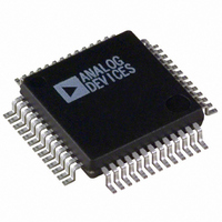
ADUC841BSZ62-5 Analog Devices Inc, ADUC841BSZ62-5 Datasheet - Page 7

ADUC841BSZ62-5
Manufacturer Part Number
ADUC841BSZ62-5
Description
IC ADC/DAC 12BIT W/MCU 52-MQFP
Manufacturer
Analog Devices Inc
Series
MicroConverter® ADuC8xxr
Datasheet
1.EVAL-ADUC842QS.pdf
(88 pages)
Specifications of ADUC841BSZ62-5
Core Size
8-Bit
Program Memory Size
62KB (62K x 8)
Core Processor
8052
Speed
20MHz
Connectivity
I²C, SPI, UART/USART
Peripherals
DMA, PSM, PWM, Temp Sensor, WDT
Number Of I /o
32
Program Memory Type
FLASH
Ram Size
2.25K x 8
Voltage - Supply (vcc/vdd)
4.75 V ~ 5.25 V
Data Converters
A/D 8x12b, D/A 2x12b
Oscillator Type
Internal
Operating Temperature
-40°C ~ 85°C
Package / Case
52-MQFP, 52-PQFP
Controller Family/series
(8051) 8052
No. Of I/o's
32
Ram Memory Size
2.25KB
Cpu Speed
20MIPS
No. Of Timers
3
No. Of Pwm Channels
2
Embedded Interface Type
UART
Rohs Compliant
Yes
Cpu Family
ADuC8xx
Device Core
8052
Device Core Size
8b
Frequency (max)
20MHz
Interface Type
I2C/SPI/UART
Total Internal Ram Size
2.25KB
# I/os (max)
34
Number Of Timers - General Purpose
3
Operating Supply Voltage (typ)
5V
Operating Supply Voltage (max)
5.25V
Operating Supply Voltage (min)
4.75V
On-chip Adc
8-chx12-bit
On-chip Dac
2-chx12-bit
Instruction Set Architecture
CISC
Operating Temp Range
-40C to 85C
Operating Temperature Classification
Industrial
Mounting
Surface Mount
Pin Count
52
Package Type
MQFP
Lead Free Status / RoHS Status
Lead free / RoHS Compliant
For Use With
EVAL-ADUC841QSZ - KIT DEV FOR ADUC841 QUICK START
Eeprom Size
-
Lead Free Status / Rohs Status
Compliant
Available stocks
Company
Part Number
Manufacturer
Quantity
Price
Company:
Part Number:
ADUC841BSZ62-5
Manufacturer:
Analog Devices Inc
Quantity:
135
Company:
Part Number:
ADUC841BSZ62-5
Manufacturer:
Analog Devices Inc
Quantity:
10 000
1
2
3
4
5
6
7
8
9
10
11
12
13
14
15
16
17
18
19
20
21
Temperature Range –40°C to +85°C.
ADC linearity is guaranteed during normal MicroConverter core operation.
ADC LSB size = V
These numbers are not production tested but are supported by design and/or characterization data on production release.
Offset and gain error and offset and gain error match are measured after factory calibration.
Based on external ADC system components, the user may need to execute a system calibration to remove additional external channel errors to achieve these
specifications.
SNR calculation includes distortion and noise components.
Channel-to-channel crosstalk is measured on adjacent channels.
The temperature monitor gives a measure of the die temperature directly; air temperature can be inferred from this result.
unbuffered mode tested with OP270 external buffer, which has a low input leakage current.
chosen for the C
with junction temperature as shown in Figure 38 in the Flash/EE Memory Reliability section.
DAC linearity is calculated using:
DAC differential nonlinearity specified on 0 V to V
DAC specification for output impedance in the unbuffered case depends on DAC code.
DAC specifications for I
Measured with C
When using an external reference device, the internal band gap reference input can be bypassed by setting the ADCCON1.6 bit.
Flash/EE memory reliability characteristics apply to both the Flash/EE program memory and the Flash/EE data memory.
Endurance is qualified to 100,000 cycles as per JEDEC Std. 22 method A117 and measured at –40°C, +25°C, and +85°C. Typical endurance at 25°C is 700,000 cycles.
Retention lifetime equivalent at junction temperature (T
Power supply current consumption is measured in normal, idle, and power-down modes under the following conditions:
DV
Power supply currents are production tested at 5.25 V and 3.3 V for a 5 V and 3 V part, respectively.
DD
Reduced code range of 100 to 4095, 0 V to V
Reduced code range of 100 to 3945, 0 V to V
DAC output load = 10 kΩ and 100 pF.
Normal Mode:
Idle Mode:
Power-Down Mode:
power supply current increases typically by 3 mA (3 V operation) and 10 mA (5 V operation) during a Flash/EE memory program or erase cycle.
REF
REF
REF
/2
pin.
pin decoupled with 0.47 µF capacitor to ground. Power-up time for the internal reference is determined by the value of the decoupling capacitor
12
, i.e., for internal V
SINK
, voltage output settling time, and digital-to-analog glitch energy depend on external buffer implementation in unbuffered mode. DAC in
software loop.
Reset = 0.4 V, digital I/O pins = open circuit, Core Clk changed via CD bits in PLLCON (ADuC842/ADuC843), PCON.0 = 1, core execution
suspended in idle mode.
Reset = 0.4 V, all Port 0 pins = 0.4 V, All other digital I/O and Port 1 pins are open circuit, Core Clk changed via CD bits in PLLCON
(ADuC842/ADuC843), PCON.0 = 1, core execution suspended in power-down mode, OSC turned on or off via OSC_PD bit (PLLCON.7) in
PLLCON SFR (ADuC842/ADuC843).
Reset = 0.4 V, digital I/O pins = open circuit, Core Clk changed via CD bits in PLLCON (ADuC842/ADuC843), core executing internal
REF
= 2.5 V, 1 LSB = 610 µV, and for external V
REF
DD
REF
range.
range.
and 0 V to V
J
) = 55°C as per JEDEC Std. 22 method A117. Retention lifetime based on an activation energy of 0.6 eV derates
DD
ranges.
Rev. 0 | Page 7 of 88
REF
= 1 V, 1 LSB = 244 µV.
ADuC841/ADuC842/ADuC843


