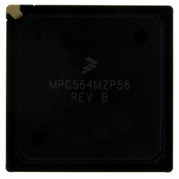
MPC564MZP56 Freescale Semiconductor, MPC564MZP56 Datasheet - Page 1213

MPC564MZP56
Manufacturer Part Number
MPC564MZP56
Description
IC MCU 512K FLASH 56MHZ 388-BGA
Manufacturer
Freescale Semiconductor
Series
MPC5xxr
Specifications of MPC564MZP56
Core Processor
PowerPC
Core Size
32-Bit
Speed
56MHz
Connectivity
CAN, EBI/EMI, SCI, SPI, UART/USART
Peripherals
POR, PWM, WDT
Number Of I /o
56
Program Memory Size
512KB (512K x 8)
Program Memory Type
FLASH
Ram Size
32K x 8
Voltage - Supply (vcc/vdd)
2.5 V ~ 2.7 V
Data Converters
A/D 32x10b
Oscillator Type
External
Operating Temperature
-40°C ~ 125°C
Package / Case
388-BGA
Core
PowerPC
Processor Series
MPC5xx
Data Bus Width
32 bit
Maximum Clock Frequency
56 MHz
Data Ram Size
32 KB
On-chip Adc
Yes
Number Of Programmable I/os
56
Number Of Timers
2
Operating Supply Voltage
0 V to 5 V
Mounting Style
SMD/SMT
A/d Bit Size
10 bit
A/d Channels Available
32
Height
1.95 mm
Interface Type
CAN, JTAG, QSPI, SCI, SPI, UART
Length
27 mm
Maximum Operating Temperature
+ 125 C
Minimum Operating Temperature
- 40 C
Supply Voltage (max)
2.7 V, 5.25 V
Supply Voltage (min)
2.5 V, 4.75 V
Width
27 mm
For Use With
MPC564EVB - KIT EVAL FOR MPC561/562/563/564
Lead Free Status / RoHS Status
Contains lead / RoHS non-compliant
Eeprom Size
-
Lead Free Status / Rohs Status
No RoHS Version Available
Available stocks
Company
Part Number
Manufacturer
Quantity
Price
Company:
Part Number:
MPC564MZP56
Manufacturer:
FREESCAL
Quantity:
364
Company:
Part Number:
MPC564MZP56
Manufacturer:
Freescale Semiconductor
Quantity:
10 000
Part Number:
MPC564MZP56
Manufacturer:
FREESCALE
Quantity:
20 000
Company:
Part Number:
MPC564MZP56R2
Manufacturer:
Freescale Semiconductor
Quantity:
10 000
- Current page: 1213 of 1420
- Download datasheet (11Mb)
Appendix E
Memory Access Timing
Table E-1
clock values show the number of clocks from the moment an address is valid on a specific bus, until data
is back on that same bus. The following assumptions were used when compiling the information:
Freescale Semiconductor
1
2
3
4
5
RCPU Load/Store
RCPU Instruction Fetches
Peripheral Mode
(only external master is
active)
Slave Mode
(both external and
internal CPUs are active)
•
•
•
•
N is the number of read cycle clocks from external address valid till external data valid. In the case of zero wait states, N
= 2.
Assuming BBC is parked on the U-bus
SIUMCR[BURST_EN] = 1
Until address is valid on external pins
“/” indicates on/off page Flash access.
The arbitration time was ignored. The values assume that the bus (or buses) involved in a
transaction was in the IDLE state when the transaction needs that bus.
The UIMB works in a mode of 1:1. This is relevant for IMB access values. In the case of 2:1 mode,
the clock latency for a cycle on the IMB should be doubled (each IMB access takes two clocks).
The basic delay of an external bus to a U-bus is four clocks (external master case).
All IMB accesses are assumed to be 16-bit accesses only. If 32-bit accesses are used, then each such
IMB access is split into two separate 16-bit cycles with normal IMB performance for each.
lists all possible memory access timings for internal and external memory combinations. The
Table E-1. Memory Access Times Using Different Buses
2-1-1-1-1..
Flash
3/4
4/5
5/6
1
MPC561/MPC563 Reference Manual, Rev. 1.2
RAM
3
1
6
7
Internal Buses
3
DECRA
M
2
6
6
IMB
—
6
7
8
SIU
1
5
6
7
4
External
Memory
Mapped
Internal
External RAM/Flash
4+N
2+N
2
Non-mappe
d Internal
Memory
4+N
2+N
Write Read
Show Cycle
—
2
1
2
5
E-1
Related parts for MPC564MZP56
Image
Part Number
Description
Manufacturer
Datasheet
Request
R

Part Number:
Description:
MPC5 1K0 5%
Manufacturer:
TE Connectivity
Datasheet:

Part Number:
Description:
MPC5 500R 5%
Manufacturer:
TE Connectivity
Datasheet:

Part Number:
Description:
MPC5 5K0 5%
Manufacturer:
Tyco Electronics
Datasheet:

Part Number:
Description:
MPC5 5R0 5%
Manufacturer:
Tyco Electronics
Datasheet:

Part Number:
Description:
MPC5 50K 5%
Manufacturer:
Tyco Electronics
Datasheet:

Part Number:
Description:
MPC5 1R0 5%
Manufacturer:
Tyco Electronics
Datasheet:
Part Number:
Description:
Manufacturer:
Freescale Semiconductor, Inc
Datasheet:
Part Number:
Description:
Manufacturer:
Freescale Semiconductor, Inc
Datasheet:
Part Number:
Description:
Manufacturer:
Freescale Semiconductor, Inc
Datasheet:
Part Number:
Description:
Manufacturer:
Freescale Semiconductor, Inc
Datasheet:
Part Number:
Description:
Manufacturer:
Freescale Semiconductor, Inc
Datasheet:


