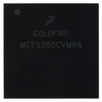
MCF5280CVM66 Freescale Semiconductor, MCF5280CVM66 Datasheet - Page 109

MCF5280CVM66
Manufacturer Part Number
MCF5280CVM66
Description
IC MPU 32BIT COLDF 256-MAPBGA
Manufacturer
Freescale Semiconductor
Series
MCF528xr
Datasheet
1.MCF5216CVM66J.pdf
(766 pages)
Specifications of MCF5280CVM66
Core Processor
Coldfire V2
Core Size
32-Bit
Speed
66MHz
Connectivity
CAN, EBI/EMI, Ethernet, I²C, SPI, UART/USART
Peripherals
DMA, LVD, POR, PWM, WDT
Number Of I /o
142
Program Memory Type
ROMless
Ram Size
64K x 8
Voltage - Supply (vcc/vdd)
2.7 V ~ 3.6 V
Data Converters
A/D 8x10b
Oscillator Type
External
Operating Temperature
-40°C ~ 85°C
Package / Case
256-MAPBGA
Controller Family/series
ColdFire
No. Of I/o's
150
Program Memory Size
2KB
Ram Memory Size
64KB
Cpu Speed
66.67MHz
Embedded Interface Type
CAN, I2C, SPI, UART
No. Of Pwm Channels
8
Rohs Compliant
Yes
Lead Free Status / RoHS Status
Lead free / RoHS Compliant
Eeprom Size
-
Program Memory Size
-
Available stocks
Company
Part Number
Manufacturer
Quantity
Price
Company:
Part Number:
MCF5280CVM66
Manufacturer:
FREESCAL
Quantity:
151
Company:
Part Number:
MCF5280CVM66
Manufacturer:
Freescale Semiconductor
Quantity:
10 000
Company:
Part Number:
MCF5280CVM66J
Manufacturer:
Freescale Semiconductor
Quantity:
10 000
Company:
Part Number:
MCF5280CVM66L
Manufacturer:
FREESCAL
Quantity:
151
- Current page: 109 of 766
- Download datasheet (9Mb)
Chapter 5
Static RAM (SRAM)
5.1
5.2
The SRAM module provides a general-purpose memory block that the ColdFire processor can access in a
single cycle. The location of the memory block can be specified to any 0-modulo-64K address within the
4-GByte address space. The memory is ideal for storing critical code or data structures or for use as the
system stack. Because the SRAM module is physically connected to the processor's high-speed local bus,
it can service processor-initiated access or memory-referencing commands from the debug module.
Depending on configuration information, instruction fetches may be sent to both the cache and the SRAM
block simultaneously. If the reference is mapped into the region defined by the SRAM, the SRAM
provides the data back to the processor, and the cache data discarded. Accesses from the SRAM module
are not cached.
The SRAM is dual-ported to provide DMA access. The SRAM is partitioned into two physical memory
arrays to allow simultaneous access to both arrays by the processor core and another bus master. See
Chapter 8, “System Control Module
5.3
The SRAM programming model includes a description of the SRAM base address register (RAMBAR),
SRAM initialization, and power management.
5.3.1
The configuration information in the SRAM base address register (RAMBAR) controls the operation of
the SRAM module.
Freescale Semiconductor
•
•
•
•
•
•
•
•
•
One 64-Kbyte SRAM
Single-cycle access
Physically located on processor's high-speed local bus
Memory location programmable on any 0-modulo-64 Kbyte address
Byte, word, longword address capabilities
The RAMBAR holds the base address of the SRAM. The MOVEC instruction provides write-only
access to this register.
The RAMBAR can be read or written from the debug module in a similar manner.
All undefined bits in the register are reserved. These bits are ignored during writes to the
RAMBAR, and return zeroes when read from the debug module.
The RAMBAR valid bit is cleared by reset, disabling the SRAM module. All other bits are
unaffected.
SRAM Features
SRAM Operation
SRAM Programming Model
SRAM Base Address Register (RAMBAR)
MCF5282 and MCF5216 ColdFire Microcontroller User’s Manual, Rev. 3
(SCM)” for more information.
5-1
Related parts for MCF5280CVM66
Image
Part Number
Description
Manufacturer
Datasheet
Request
R
Part Number:
Description:
Manufacturer:
Freescale Semiconductor, Inc
Datasheet:
Part Number:
Description:
Manufacturer:
Freescale Semiconductor, Inc
Datasheet:
Part Number:
Description:
Manufacturer:
Freescale Semiconductor, Inc
Datasheet:
Part Number:
Description:
Manufacturer:
Freescale Semiconductor, Inc
Datasheet:
Part Number:
Description:
Manufacturer:
Freescale Semiconductor, Inc
Datasheet:
Part Number:
Description:
Manufacturer:
Freescale Semiconductor, Inc
Datasheet:
Part Number:
Description:
Manufacturer:
Freescale Semiconductor, Inc
Datasheet:
Part Number:
Description:
Manufacturer:
Freescale Semiconductor, Inc
Datasheet:
Part Number:
Description:
Manufacturer:
Freescale Semiconductor, Inc
Datasheet:
Part Number:
Description:
Manufacturer:
Freescale Semiconductor, Inc
Datasheet:
Part Number:
Description:
Manufacturer:
Freescale Semiconductor, Inc
Datasheet:
Part Number:
Description:
Manufacturer:
Freescale Semiconductor, Inc
Datasheet:
Part Number:
Description:
Manufacturer:
Freescale Semiconductor, Inc
Datasheet:
Part Number:
Description:
Manufacturer:
Freescale Semiconductor, Inc
Datasheet:
Part Number:
Description:
Manufacturer:
Freescale Semiconductor, Inc
Datasheet:


