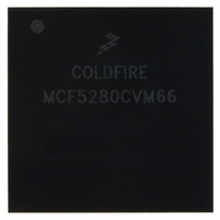
MCF5280CVM66 Freescale Semiconductor, MCF5280CVM66 Datasheet - Page 290

MCF5280CVM66
Manufacturer Part Number
MCF5280CVM66
Description
IC MPU 32BIT COLDF 256-MAPBGA
Manufacturer
Freescale Semiconductor
Series
MCF528xr
Datasheet
1.MCF5216CVM66J.pdf
(766 pages)
Specifications of MCF5280CVM66
Core Processor
Coldfire V2
Core Size
32-Bit
Speed
66MHz
Connectivity
CAN, EBI/EMI, Ethernet, I²C, SPI, UART/USART
Peripherals
DMA, LVD, POR, PWM, WDT
Number Of I /o
142
Program Memory Type
ROMless
Ram Size
64K x 8
Voltage - Supply (vcc/vdd)
2.7 V ~ 3.6 V
Data Converters
A/D 8x10b
Oscillator Type
External
Operating Temperature
-40°C ~ 85°C
Package / Case
256-MAPBGA
Controller Family/series
ColdFire
No. Of I/o's
150
Program Memory Size
2KB
Ram Memory Size
64KB
Cpu Speed
66.67MHz
Embedded Interface Type
CAN, I2C, SPI, UART
No. Of Pwm Channels
8
Rohs Compliant
Yes
Lead Free Status / RoHS Status
Lead free / RoHS Compliant
Eeprom Size
-
Program Memory Size
-
Available stocks
Company
Part Number
Manufacturer
Quantity
Price
Company:
Part Number:
MCF5280CVM66
Manufacturer:
FREESCAL
Quantity:
151
Company:
Part Number:
MCF5280CVM66
Manufacturer:
Freescale Semiconductor
Quantity:
10 000
Company:
Part Number:
MCF5280CVM66J
Manufacturer:
Freescale Semiconductor
Quantity:
10 000
Company:
Part Number:
MCF5280CVM66L
Manufacturer:
FREESCAL
Quantity:
151
- Current page: 290 of 766
- Download datasheet (9Mb)
Synchronous DRAM Controller Module
15.2.4.1 Mode Register Settings
It is possible to configure the operation of SDRAMs, namely their burst operation and CAS latency,
through the SDRAM component’s mode register. CAS latency is a function of the speed of the SDRAM
and the bus clock of the DRAM controller. The DRAM controller operates at a CAS latency of 1, 2, or 3.
Although the DRAM controller supports bursting operations, it does not use the bursting features of the
SDRAMs. Because the processor can burst operand sizes of 1, 2, 4, or 16 bytes long, the concept of a fixed
burst length in the SDRAMs mode register becomes problematic. Therefore, the processor DRAM
controller generates the burst cycles rather than the SDRAM device. Because the processor generates a
new address and a
should be set either not to burst or to a burst length of one. This allows bursting to be controlled by the
processor.
The SDRAM mode register is written by setting the associated block’s DACR[IMRS]. First, the base
address and mask registers must be set to the appropriate configuration to allow the mode register to be
set. Note that improperly set DMR mask bits may prevent access to the mode register address. Thus, the
user should determine the mapping of the mode register address to the processor address bits to find out if
an access is blocked. If the DMR setting prohibits mode register access, the DMR should be reconfigured
to enable the access and then set to its necessary configuration after the
The associated CBM bits should also be initialized. After DACR[IMRS] is set, the next access to the
SDRAM address space generates the
selected to place the correct mode information on the SDRAM address pins. The address is not multiplexed
for the
of that access needs the correct mode programming information on the correct address bits.
Figure 15-10
15.3
This example interfaces a 512K x 32-bit x 4 bank SDRAM component to processor operating at 40 MHz.
Table 15-25
15-18
MRS
SDRAM Example
command. The
lists design specifications for this example.
shows the
READ
MRS
MCF5282 and MCF5216 ColdFire Microcontroller User’s Manual, Rev. 3
or
MRS
WRITE
SD_CS[1] or [0]
Figure 15-10. Mode Register Set (
command, which occurs in the first clock of the bus cycle.
SRAS, SCAS
access can be a read or write. The important thing is that the address output
CLKOUT
DRAMW
command for each transfer within the burst, the SDRAM mode register
D[31:0]
A[23:0]
MRS
command to that SDRAM. The address of the access should be
MRS
MRS
) Command
MRS
command executes.
Freescale Semiconductor
Related parts for MCF5280CVM66
Image
Part Number
Description
Manufacturer
Datasheet
Request
R
Part Number:
Description:
Manufacturer:
Freescale Semiconductor, Inc
Datasheet:
Part Number:
Description:
Manufacturer:
Freescale Semiconductor, Inc
Datasheet:
Part Number:
Description:
Manufacturer:
Freescale Semiconductor, Inc
Datasheet:
Part Number:
Description:
Manufacturer:
Freescale Semiconductor, Inc
Datasheet:
Part Number:
Description:
Manufacturer:
Freescale Semiconductor, Inc
Datasheet:
Part Number:
Description:
Manufacturer:
Freescale Semiconductor, Inc
Datasheet:
Part Number:
Description:
Manufacturer:
Freescale Semiconductor, Inc
Datasheet:
Part Number:
Description:
Manufacturer:
Freescale Semiconductor, Inc
Datasheet:
Part Number:
Description:
Manufacturer:
Freescale Semiconductor, Inc
Datasheet:
Part Number:
Description:
Manufacturer:
Freescale Semiconductor, Inc
Datasheet:
Part Number:
Description:
Manufacturer:
Freescale Semiconductor, Inc
Datasheet:
Part Number:
Description:
Manufacturer:
Freescale Semiconductor, Inc
Datasheet:
Part Number:
Description:
Manufacturer:
Freescale Semiconductor, Inc
Datasheet:
Part Number:
Description:
Manufacturer:
Freescale Semiconductor, Inc
Datasheet:
Part Number:
Description:
Manufacturer:
Freescale Semiconductor, Inc
Datasheet:


