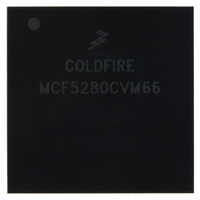
MCF5280CVM66 Freescale Semiconductor, MCF5280CVM66 Datasheet - Page 302

MCF5280CVM66
Manufacturer Part Number
MCF5280CVM66
Description
IC MPU 32BIT COLDF 256-MAPBGA
Manufacturer
Freescale Semiconductor
Series
MCF528xr
Datasheet
1.MCF5216CVM66J.pdf
(766 pages)
Specifications of MCF5280CVM66
Core Processor
Coldfire V2
Core Size
32-Bit
Speed
66MHz
Connectivity
CAN, EBI/EMI, Ethernet, I²C, SPI, UART/USART
Peripherals
DMA, LVD, POR, PWM, WDT
Number Of I /o
142
Program Memory Type
ROMless
Ram Size
64K x 8
Voltage - Supply (vcc/vdd)
2.7 V ~ 3.6 V
Data Converters
A/D 8x10b
Oscillator Type
External
Operating Temperature
-40°C ~ 85°C
Package / Case
256-MAPBGA
Controller Family/series
ColdFire
No. Of I/o's
150
Program Memory Size
2KB
Ram Memory Size
64KB
Cpu Speed
66.67MHz
Embedded Interface Type
CAN, I2C, SPI, UART
No. Of Pwm Channels
8
Rohs Compliant
Yes
Lead Free Status / RoHS Status
Lead free / RoHS Compliant
Eeprom Size
-
Program Memory Size
-
Available stocks
Company
Part Number
Manufacturer
Quantity
Price
Company:
Part Number:
MCF5280CVM66
Manufacturer:
FREESCAL
Quantity:
151
Company:
Part Number:
MCF5280CVM66
Manufacturer:
Freescale Semiconductor
Quantity:
10 000
Company:
Part Number:
MCF5280CVM66J
Manufacturer:
Freescale Semiconductor
Quantity:
10 000
Company:
Part Number:
MCF5280CVM66L
Manufacturer:
FREESCAL
Quantity:
151
- Current page: 302 of 766
- Download datasheet (9Mb)
DMA Controller Module
16.4.2
DARn, shown in
16-6
Address
Address
Reset
Reset
Field
Field
R/W
R/W
Destination Address Registers (DAR0–DAR3)
31
31
The backdoor enable bit must be set in both the core and SCM in order to
enable backdoor accesses from the DMA to SRAM. See
“Memory Base Address Register
Flash accesses (reads/writes) by a bus master other than the core (DMA
controller or Fast Ethernet Controller), or writes to Flash by the core during
programming, must use the backdoor Flash address of IPSBAR plus an
offset of 0x0400_0000. For example, for a DMA transfer from the first
Flash location when IPSBAR is still at its default location of 0x4000_0000,
the source register would be loaded with 0x4400_0000. Backdoor Flash
read accesses can be made with the bus master, but it takes two cycles longer
than a direct read of the Flash when using the FLASHBAR address.
The DMA does not maintain coherency with the cache. Therefore, DMAs
should not transfer data to cacheable memory unless software is used to
maintain the cache coherency.
The DMA should not be used to write data to the UART transmit FIFO in
cycle steal mode. When the UART interrupt is used as a DMA request it
does not negate fast enough to get a single transfer. The UART transmit
FIFO only has one entry so the data from the second byte would be lost.
Figure
MCF5282 and MCF5216 ColdFire Microcontroller User’s Manual, Rev. 3
16-5, holds the address to which the DMA controller sends data.
Figure 16-5. Destination Address Registers (DARn)
Figure 16-4. Source Address Registers (SARn)
0000_0000_0000_0000_0000_0000_0000_0000
0000_0000_0000_0000_0000_0000_0000_0000
IPSBAR + 0x100, 0x140, 0x180, 0x1C0
IPSBAR + 0x104, 0x144, 0x184, 0x1C4
(RAMBAR)” for more details.
NOTE
NOTE
NOTE
NOTE
SAR
DAR
R/W
R/W
Section 8.4.2,
Freescale Semiconductor
0
0
Related parts for MCF5280CVM66
Image
Part Number
Description
Manufacturer
Datasheet
Request
R
Part Number:
Description:
Manufacturer:
Freescale Semiconductor, Inc
Datasheet:
Part Number:
Description:
Manufacturer:
Freescale Semiconductor, Inc
Datasheet:
Part Number:
Description:
Manufacturer:
Freescale Semiconductor, Inc
Datasheet:
Part Number:
Description:
Manufacturer:
Freescale Semiconductor, Inc
Datasheet:
Part Number:
Description:
Manufacturer:
Freescale Semiconductor, Inc
Datasheet:
Part Number:
Description:
Manufacturer:
Freescale Semiconductor, Inc
Datasheet:
Part Number:
Description:
Manufacturer:
Freescale Semiconductor, Inc
Datasheet:
Part Number:
Description:
Manufacturer:
Freescale Semiconductor, Inc
Datasheet:
Part Number:
Description:
Manufacturer:
Freescale Semiconductor, Inc
Datasheet:
Part Number:
Description:
Manufacturer:
Freescale Semiconductor, Inc
Datasheet:
Part Number:
Description:
Manufacturer:
Freescale Semiconductor, Inc
Datasheet:
Part Number:
Description:
Manufacturer:
Freescale Semiconductor, Inc
Datasheet:
Part Number:
Description:
Manufacturer:
Freescale Semiconductor, Inc
Datasheet:
Part Number:
Description:
Manufacturer:
Freescale Semiconductor, Inc
Datasheet:
Part Number:
Description:
Manufacturer:
Freescale Semiconductor, Inc
Datasheet:


