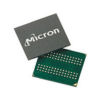
MT46H16M32LFCM-6:B Micron Technology Inc, MT46H16M32LFCM-6:B Datasheet - Page 24

MT46H16M32LFCM-6:B
Manufacturer Part Number
MT46H16M32LFCM-6:B
Description
Manufacturer
Micron Technology Inc
Type
DDR SDRAMr
Datasheet
1.MT46H16M32LFCM-6B.pdf
(98 pages)
Specifications of MT46H16M32LFCM-6:B
Organization
16Mx32
Density
512Mb
Address Bus
15b
Access Time (max)
6.5/5ns
Maximum Clock Rate
166MHz
Operating Supply Voltage (typ)
1.8V
Package Type
VFBGA
Operating Temp Range
0C to 70C
Operating Supply Voltage (max)
1.95V
Operating Supply Voltage (min)
1.7V
Supply Current
115mA
Pin Count
90
Mounting
Surface Mount
Operating Temperature Classification
Commercial
Lead Free Status / RoHS Status
Compliant
Available stocks
Company
Part Number
Manufacturer
Quantity
Price
Company:
Part Number:
MT46H16M32LFCM-6:B
Manufacturer:
MICRON
Quantity:
4 000
Company:
Part Number:
MT46H16M32LFCM-6:B TR
Manufacturer:
Micron Technology Inc
Quantity:
10 000
Table 10: I
Notes 1–5, 7, and 12 apply to all parameters/conditions in this table; V
PDF: 09005aef82d5d305
512mb_ddr_mobile_sdram_t47m.pdf – Rev. I 12/09 EN
Parameter/Condition
Self refresh
CKE = LOW;
inputs are stable; Data bus inputs are stable
DD6
t
CK =
Specifications and Conditions
t
CK (MIN); Address and control
Notes:
10. CKE must be active (HIGH) during the entire time a REFRESH command is executed.
11. This limit is a nominal value and does not result in a fail. CKE is HIGH during REFRESH
12. Values for I
13. Typical values at 25˚C, not a maximum value.
1. All voltages referenced to V
2. Tests for I
3. Timing and I
4. I
5. I
6. MIN (
7. Measurement is taken 500ms after entering into this operating mode to allow settling
8. V
9. I
related specifications and device operation are guaranteed for the full voltage range
specified.
but input timing is still referenced to V
output timing reference voltage level is V
minimum cycle time with the outputs open.
aged at the defined cycle rate.
minimum absolute value for the respective parameter.
ments is the largest multiple of
time for the tester.
From the time the AUTO REFRESH command is registered, CKE must be active at each
rising clock edge until
command period (
ues are estimated.
DD
DD
DD2N
DD
is dependent on output loading and cycle rates. Specified values are obtained with
specifications are tested after the device is properly initialized and values are aver-
must not vary more than 4% if CKE is not active while any bank is active.
t
specifies DQ, DQS, and DM to be driven to a valid high or low logic level.
RC or
DD
DD6
t
characteristics may be conducted at nominal supply voltage levels, but the
DD
RFC) for I
85˚C are guaranteed for the entire temperature range. All other I
tests may use a V
t
RFC [MIN]) else CKE is LOW (for example, during standby).
1/16 array, 85˚C
1/16 array, 45˚C
Full array, 85˚C
Full array, 45˚C
1/2 array, 85˚C
1/2 array, 45˚C
1/4 array, 85˚C
1/4 array, 45˚C
1/8 array, 85˚C
1/8 array, 45˚C
DD
t
RFC later.
measurements is the smallest multiple of
24
SS
Electrical Specifications – I
.
512Mb: x16, x32 Mobile LPDDR SDRAM
t
CK that meets the maximum absolute value for
IL
-to-V
DD
Micron Technology, Inc. reserves the right to change products or specifications without notice.
/V
IH
DDQ
DDQ
swing of up to 1.5V in the test environment,
Symbol
DDQ
/2 (or to the crossing point for CK/CK#). The
I
= 1.70–1.95V
DD6
/2.
Low Power
t
RAS (MAX) for I
500
250
400
220
350
205
350
205
325
200
© 2004 Micron Technology, Inc. All rights reserved.
t
CK that meets the
DD
Standard
DD
Parameters
700
390
520
310
430
275
430
275
375
250
measure-
t
DD6
RAS.
Units
μA
μA
μA
μA
μA
μA
μA
μA
μA
μA
val-


