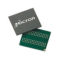
MT46H16M32LFCM-6:B Micron Technology Inc, MT46H16M32LFCM-6:B Datasheet - Page 28

MT46H16M32LFCM-6:B
Manufacturer Part Number
MT46H16M32LFCM-6:B
Description
Manufacturer
Micron Technology Inc
Type
DDR SDRAMr
Datasheet
1.MT46H16M32LFCM-6B.pdf
(98 pages)
Specifications of MT46H16M32LFCM-6:B
Organization
16Mx32
Density
512Mb
Address Bus
15b
Access Time (max)
6.5/5ns
Maximum Clock Rate
166MHz
Operating Supply Voltage (typ)
1.8V
Package Type
VFBGA
Operating Temp Range
0C to 70C
Operating Supply Voltage (max)
1.95V
Operating Supply Voltage (min)
1.7V
Supply Current
115mA
Pin Count
90
Mounting
Surface Mount
Operating Temperature Classification
Commercial
Lead Free Status / RoHS Status
Compliant
Available stocks
Company
Part Number
Manufacturer
Quantity
Price
Company:
Part Number:
MT46H16M32LFCM-6:B
Manufacturer:
MICRON
Quantity:
4 000
Company:
Part Number:
MT46H16M32LFCM-6:B TR
Manufacturer:
Micron Technology Inc
Quantity:
10 000
Table 11: Electrical Characteristics and Recommended AC Operating Conditions (Continued)
Notes 1–9 apply to all parameters in this table; V
PDF: 09005aef82d5d305
512mb_ddr_mobile_sdram_t47m.pdf – Rev. I 12/09 EN
Parameter
DQS read postamble
Active bank a to active bank b
command
Read of SRR to next valid
command
SRR to read
DQS write preamble
DQS write preamble setup time
DQS write postamble
Write recovery time
Internal WRITE-to-READ
command delay
Exit power-down mode to first
valid command
Exit self refresh to first valid
command
Notes:
1. All voltages referenced to V
2. All parameters assume proper device initialization.
3. Tests for AC timing and electrical AC and DC characteristics may be conducted at nomi-
4. The circuit shown below represents the timing reference load used in defining the rele-
5. The CK/CK# input reference voltage level (for timing referenced to CK/CK#) is the point
6. A CK and CK# input slew rate ≥1 V/ns (2 V/ns if measured differentially) is assumed for
7. All AC timings assume an input slew rate of 1 V/ns.
nal supply voltage levels, but the related specifications and device operation are guaran-
teed for the full voltage ranges specified.
vant timing parameters of the device. It is not intended to be either a precise representa-
tion of the typical system environment or a depiction of the actual load presented by a
production tester. System designers will use IBIS or other simulation tools to correlate
the timing reference load to system environment. Specifications are correlated to produc-
tion test conditions (generally a coaxial transmission line terminated at the tester elec-
tronics). For the half-strength driver with a nominal 10pF load, parameters
are expected to be in the same range. However, these parameters are not subject to
production test but are estimated by design/characterization. Use of IBIS or other simula-
tion tools for system design validation is suggested.
at which CK and CK# cross; the input reference voltage level for signals other than CK/
CK# is V
all parameters.
Symbol
t
t
WPRES
t
t
I/O
WPRE
t
t
WPST
t
t
t
RPST
t
WTR
RRD
t
XSR
SRC
SRR
WR
XP
Full drive strength
DDQ
CL + 1
50
Min
0.25
/2.
120
0.4
0.4
10
15
2
0
2
2
Electrical Specifications – AC Operating Conditions
DD
/V
-5
DDQ
Max
0.6
0.6
–
–
–
–
–
–
–
–
–
20pF
= 1.70–1.95V
28
CL + 1
Min
10.8
0.25
120
0.4
0.4
SS
15
2
0
2
2
.
I/O
512Mb: x16, x32 Mobile LPDDR SDRAM
-54
Half drive strength
Max
0.6
0.6
Micron Technology, Inc. reserves the right to change products or specifications without notice.
–
–
–
–
–
–
–
–
–
50
CL + 1
Min
0.25
120
0.4
0.4
12
15
2
0
2
1
-6
Max
10pF
0.6
0.6
–
–
–
–
–
–
–
–
–
CL + 1
Min
0.25
120
0.4
0.4
15
15
© 2004 Micron Technology, Inc. All rights reserved.
2
0
1
1
-75
Max
0.6
0.6
–
–
–
–
–
–
–
–
–
Unit Notes
t
t
t
t
t
t
t
t
AC and
CK
ns
CK
CK
CK
ns
CK
ns
CK
CK
ns
23, 24
25
26
27
t
QH


