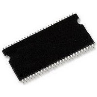
MT48LC16M16A2P-7E:D Micron Technology Inc, MT48LC16M16A2P-7E:D Datasheet - Page 14

MT48LC16M16A2P-7E:D
Manufacturer Part Number
MT48LC16M16A2P-7E:D
Description
SDRAM 256MB, SMD, 48LC16, TSOP54
Manufacturer
Micron Technology Inc
Type
SDRAMr
Series
-r
Specifications of MT48LC16M16A2P-7E:D
Organization
16Mx16
Density
256Mb
Address Bus
15b
Access Time (max)
5.4ns
Maximum Clock Rate
143MHz
Operating Supply Voltage (typ)
3.3V
Package Type
TSOP-II
Operating Temp Range
0C to 70C
Operating Supply Voltage (max)
3.6V
Operating Supply Voltage (min)
3V
Supply Current
135mA
Pin Count
54
Mounting
Surface Mount
Operating Temperature Classification
Commercial
Access Time
RoHS Compliant
Memory Case Style
TSOP
No. Of Pins
54
Operating Temperature Range
0°C To +70°C
Operating Temperature Max
70°C
Operating Temperature Min
0°C
Package / Case
TSOP
Memory Type
DRAM - Synchronous
Memory Configuration
4 BLK (4M X 16)
Interface Type
LVTTL
Rohs Compliant
Yes
Format - Memory
RAM
Memory Size
256M (16Mx16)
Speed
133MHz
Interface
Parallel
Voltage - Supply
3 V ~ 3.6 V
Operating Temperature
0°C ~ 70°C
Lead Free Status / RoHS Status
Compliant
Lead Free Status / RoHS Status
Compliant
Available stocks
Company
Part Number
Manufacturer
Quantity
Price
Company:
Part Number:
MT48LC16M16A2P-7E:D
Manufacturer:
MICRON
Quantity:
5 520
Company:
Part Number:
MT48LC16M16A2P-7E:D TR
Manufacturer:
MICRON
Quantity:
11 200
Company:
Part Number:
MT48LC16M16A2P-7E:D TR
Manufacturer:
AVAGO
Quantity:
6 700
Figure 6:
Burst Type
PDF: 09005aef80725c0b/Source: 09005aef806fc13c
64MSDRAM_2.fm - Rev. M 10/07 EN
M8
0
–
M9
0
1
Mode Register Definition
M7
0
–
Programmed Burst Length
M6–M0
Defined
Single Location Access
to ensure compatibility
–
Write Burst Mode
with future devices.
Accesses within a given burst may be programmed to be either sequential or interleaved;
this is referred to as the burst type and is selected via bit M3.
The ordering of accesses within a burst is determined by the burst length, the burst type
and the starting column address, as shown in Table 5 on page 15.
M11, M10 = “0, 0”
Operating Mode
Standard Operation
All other states reserved
BA0, BA1,
Program
Reserved WB
11
A11
10
A10
M6
0
0
0
0
1
1
1
1
9
A9
M5
Op Mode
0
0
1
1
0
0
1
1
8
M4
A8
0
1
0
1
0
1
0
1
7
A7
14
CAS Latency
6
A6
CAS Latency
5
Reserved
Reserved
Reserved
Reserved
Reserved
Reserved
A5
Micron Technology, Inc., reserves the right to change products or specifications without notice.
2
3
4
A4
M3
BT
0
1
3
A3
M2
0
0
0
0
1
1
1
1
Burst Length
2
M1
A2
0
0
1
1
0
0
1
1
M0
1
0
1
0
1
0
1
0
1
A1
64Mb: x4, x8, x16 SDRAM
0
A0
Functional Description
Reserved
Reserved
Reserved
Full Page
Burst Type
Interleaved
Sequential
3 = 0
1
2
4
8
Mode Register (Mx)
©2000 Micron Technology, Inc. All rights reserved.
Burst Length
Address Bus
Reserved
Reserved
Reserved
Reserved
M3 = 1
1
2
4
8


