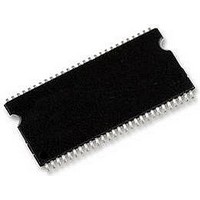
MT48LC16M16A2P-7E:D Micron Technology Inc, MT48LC16M16A2P-7E:D Datasheet - Page 48

MT48LC16M16A2P-7E:D
Manufacturer Part Number
MT48LC16M16A2P-7E:D
Description
SDRAM 256MB, SMD, 48LC16, TSOP54
Manufacturer
Micron Technology Inc
Type
SDRAMr
Series
-r
Specifications of MT48LC16M16A2P-7E:D
Organization
16Mx16
Density
256Mb
Address Bus
15b
Access Time (max)
5.4ns
Maximum Clock Rate
143MHz
Operating Supply Voltage (typ)
3.3V
Package Type
TSOP-II
Operating Temp Range
0C to 70C
Operating Supply Voltage (max)
3.6V
Operating Supply Voltage (min)
3V
Supply Current
135mA
Pin Count
54
Mounting
Surface Mount
Operating Temperature Classification
Commercial
Access Time
RoHS Compliant
Memory Case Style
TSOP
No. Of Pins
54
Operating Temperature Range
0°C To +70°C
Operating Temperature Max
70°C
Operating Temperature Min
0°C
Package / Case
TSOP
Memory Type
DRAM - Synchronous
Memory Configuration
4 BLK (4M X 16)
Interface Type
LVTTL
Rohs Compliant
Yes
Format - Memory
RAM
Memory Size
256M (16Mx16)
Speed
133MHz
Interface
Parallel
Voltage - Supply
3 V ~ 3.6 V
Operating Temperature
0°C ~ 70°C
Lead Free Status / RoHS Status
Compliant
Lead Free Status / RoHS Status
Compliant
Available stocks
Company
Part Number
Manufacturer
Quantity
Price
Company:
Part Number:
MT48LC16M16A2P-7E:D
Manufacturer:
MICRON
Quantity:
5 520
Company:
Part Number:
MT48LC16M16A2P-7E:D TR
Manufacturer:
MICRON
Quantity:
11 200
Company:
Part Number:
MT48LC16M16A2P-7E:D TR
Manufacturer:
AVAGO
Quantity:
6 700
Notes
PDF: 09005aef80725c0b/Source: 09005aef806fc13c
64MSDRAM_2.fm - Rev. M 10/07 EN
10.
11. C timing and I
12. Other input signals are allowed to transition no more than once every two clocks and
13. I
14. Timing actually specified by
15. Timing actually specified by
16. Timing actually specified by
17. Required clocks are specified by JEDEC functionality and are not dependent on any
18. The I
19. Address transitions average one transition every two clocks.
20. CLK must be toggled a minimum of two times during this period.
21. Based on
1. All voltages referenced to V
2. This parameter is sampled. V
3. I
4. Enables on-chip refresh and address counters.
5. The minimum specifications are used only to indicate cycle time at which proper
6. An initial pause of 100µs is required after power-up, followed by two AUTO REFRESH
7. AC characteristics assume
8. In addition to meeting the transition rate specification, the clock and CKE must tran-
9. Outputs measured at 1.5V with equivalent load:
biased at 1.4V.
with minimum cycle time and the outputs open.
operation over the full temperature range (0°C ≤ T
IT parts) is ensured.
commands, before proper device operation is ensured. (V
ered up simultaneously. V
REFRESH command wake-ups should be repeated any time the
ment is exceeded.
sit between V
Q
t
a reference to V
High-Z.
crossover point. If the input transition time is longer than 1 ns, then the timing is ref-
erenced at V
should always be 1.5V referenced to crossover. Refer to Micron technical note
TN-48-09.
are otherwise at valid V
cycle rate.
minimum cycle rate.
timing parameter.
frequency alteration for the test condition.
DD
HZ defines the time at which the output achieves the open circuit condition; it is not
DD
is dependent on output loading and cycle rates. Specified values are obtained
specifications are tested after the device is properly initialized.
DD
current will increase or decrease proportionally according to the amount of
t
CK = 7.5ns for -75 and -7E,
IL
IH
50pF
DD
(MAX) and V
OH
and V
tests have V
or V
IL
OL
IH
(or between V
. The last valid data element will meet
SS
or V
t
48
SS
T = 1ns.
IH
and V
t
t
t
.
DD
CKS; clock(s) specified as a reference only at minimum
WR plus
WR.
IL
(MIN) and no longer at the 1.5V crossover point. CLK
IL
= 0V and V
, V
levels.
SS
DD
Q must be at same potential.) The two AUTO
Micron Technology, Inc., reserves the right to change products or specifications without notice.
Q = +3.3V; f = 1 MHz, T
t
IL
t
CK = 6ns for -6.
RP; clock(s) specified as a reference only at
and V
IH
= 3V, with timing referenced to 1.5V
IH
) in a monotonic manner.
A
≤ +70°C and –40°C ≤ T
64Mb: x4, x8, x16 SDRAM
DD
©2000 Micron Technology, Inc. All rights reserved.
A
and V
= 25°C; pin under test
t
OH before going
t
REF refresh require-
DD
Q must be pow-
A
≤ +85°C for
Notes


