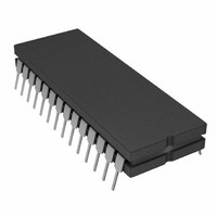
AD7878SQ Analog Devices Inc, AD7878SQ Datasheet - Page 10

AD7878SQ
Manufacturer Part Number
AD7878SQ
Description
IC ADC 12BIT W/DSP INT 28-CDIP
Manufacturer
Analog Devices Inc
Datasheet
1.AD7878JPZ-REEL.pdf
(16 pages)
Specifications of AD7878SQ
Rohs Status
RoHS non-compliant
Number Of Bits
12
Sampling Rate (per Second)
100k
Data Interface
DSP
Number Of Converters
1
Power Dissipation (max)
95.5mW
Voltage Supply Source
Analog and Digital, Dual ±
Operating Temperature
-55°C ~ 125°C
Mounting Type
Through Hole
Package / Case
28-CDIP (0.600", 15.24mm)
Available stocks
Company
Part Number
Manufacturer
Quantity
Price
Part Number:
AD7878SQ
Manufacturer:
ADI/亚德诺
Quantity:
20 000
AD7878
CONVERSION TIMING
The track-and-hold on the AD7878 goes from track-to-hold
mode on the rising edge of CONVST, and the value of V
this point is the value which will be converted. However, the
conversion actually sorts on the next rising edge of CLK IN
after CONVST goes high. If CONVST goes high within ap-
INTERNAL REFERENCE
The AD7878 has an on-chip temperature compensated buried
Zener reference (see Figure 14) that is factory trimmed to 3 V
dc bias required for bipolar operation. The reference output is
available (REF OUT) and is capable of providing up to 500 A
to an external load.
The maximum recommended capacitance on REF OUT for
normal operation is 50 pF. If the reference is required for use
external to the AD7878, it should be decoupled with a
200
tantalum capacitor and a 0.1 F ceramic capacitor. These
decoupling components are required to remove voltage spikes
caused by the internal operation of the AD7878.
TRACK-AND-HOLD AMPLIFIER
The track-and-hold amplifier on the analog input of the
AD7878 allows the ADC to accurately convert an input sine
wave of 6 V peak-peak amplitude to 12-bit accuracy. The input
bandwidth of the track/hold amplifier is much greater than the
Nyquist rate of the ADC even when operated at its minimum
conversion time. The 0.1 dB cutoff frequency occurs typically
at 500 kHz. The track/hold amplifier acquires an input signal to
12-bit accuracy in less than 2 s.
The operation of the track/hold amplifier is transparent to the
user. The track/hold amplifier goes from its tracking mode to
its hold mode at the start of conversion on the rising edge of
CONVST and returns to track mode at the end of conversion.
proximately 30 ns prior to a rising edge of CLK IN, that CLK
IN edge will not be seen as the first CLK IN edge of the con-
version process, and conversion will not actually start until one
CLK IN cycle later. As a result, the conversion time (from
CONVST to FIFO update) will vary by one clock cycle de-
pending on the relationship between CONVST and CLK IN.
A conversion cycle normally consists of 56 CLK IN cycles
(assuming no read/write operations) which corresponds to a 7
As conversion time. If CONVST goes high within 30 ns prior
to a rising edge of CLK IN, the conversion time will consist of
57 CLK IN cycles, i.e., 7.125 s. This effect does not cause
track/hold jitter.
1%. Internally, it provides both the DAC reference and the
resistor in series with a parallel combination of a 10 F
Figure 14. AD7878 Reference Circuit
IN
at
–10–
ANALOG INPUT
Figure 15 shows the AD7878 analog input. The analog input
range is 3 V into an input resistance of typically 15 k . The
designed code transitions occur midway between successive
integer LSB values (i.e., 1/2 LSB, 3/2 LSBs, 5/2 LSBs . . . .
FS–3/2 LSBs). The output code is 2s complement binary with
1 LSB = FS/4096 = 6 V/4096 = 1.46 mV. The ideal input/
output transfer function is shown in Figure 16.
OFFSET AND FULL-SCALE ADJUSTMENT
In most Digital Signal Processing (DSP) applications offset and
full-scale error have little or no effect on system performance.
Offset error can always be eliminated in the analog domain by
ac coupling. Full-scale error effect is linear and does not cause
problems as long as the input signal is within the full dynamic
range of the ADC. Some applications may require that the input
signal span the full analog input dynamic range and, accord-
ingly, offset and full-scale error will have to be adjusted to zero.
Where adjustment is required, offset must be adjusted before
full-scale error. This is achieved by trimming the offset of the
op amp driving the analog input of the AD7878 while the input
voltage is 1/2 LSB below ground. The trim procedure is as
follows: apply a voltage of –0.73 mV (–1/2 LSB) at V
adjust the op amp offset voltage until the ADC output code
flickers between 1111 1111 1111 and 0000 0000 0000.
Gain error can be adjusted at either the first code transition
(ADC negative full scale) or the last code transition (ADC
positive full scale). The trim procedures for both cases are as
follows:
Figure 16. Input/Output Transfer Function
Figure 15. AD7878 Analog Input
1
and
REV. A


