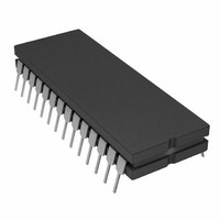
AD7878SQ Analog Devices Inc, AD7878SQ Datasheet - Page 5

AD7878SQ
Manufacturer Part Number
AD7878SQ
Description
IC ADC 12BIT W/DSP INT 28-CDIP
Manufacturer
Analog Devices Inc
Datasheet
1.AD7878JPZ-REEL.pdf
(16 pages)
Specifications of AD7878SQ
Rohs Status
RoHS non-compliant
Number Of Bits
12
Sampling Rate (per Second)
100k
Data Interface
DSP
Number Of Converters
1
Power Dissipation (max)
95.5mW
Voltage Supply Source
Analog and Digital, Dual ±
Operating Temperature
-55°C ~ 125°C
Mounting Type
Through Hole
Package / Case
28-CDIP (0.600", 15.24mm)
Available stocks
Company
Part Number
Manufacturer
Quantity
Price
Part Number:
AD7878SQ
Manufacturer:
ADI/亚德诺
Quantity:
20 000
Model
AD7878JN
AD7878AQ
AD7878SQ
AD7878KN
AD7878BQ
AD7878LN
AD7878SE
AD7878JP
AD7878KP
AD7878LP
NOTES
1
2
3
4
STATUS/CONTROL REGISTER
The status/control register serves the dual function of providing
control and monitoring the status of the FIFO memory. This
register is directly accessible through the data bus (DB11–DB0)
with a read or write operation while ADD0 is high. A write
operation to the status/control register provides control for the
ALFL output, bus interface and FIFO counter reset. This is
normally done on power-up initialization. The FIFO memory
address pointer is incremented after each conversion and com-
pared with a preprogrammed count in the status/control regis-
ter. When this preprogrammed count is reached, the ALFL
output is asserted if the ENAF control bit is set to zero. This
ALFL can be used to interrupt the microprocessor after any
predetermined number of conversions (between 1 and 8). The
status of the address pointer along with sample overrange and
ALFL status can be accessed at any time by reading the status/
control register. Note: reading the status/control register does
not cause any internal data movement in the FIFO memory.
Status information for a particular word should be read from the
status register before the data word is read from the FIFO
memory.
STATUS/CONTROL REGISTER FUNCTION
DESCRIPTION
DB11 (ALFL)
Almost Full Flag, Read only. This is the same as Pin 6 (ALFL
output) status. A logic low indicates that the word count in
the FIFO memory has reached the preprogrammed count in bit
locations DB10–DB8. ALFL is updated at the end of conversion.
BIT LOCATION
STATUS INFORMATION (READ)
CONTROL FUNCTION (WRITE)
RESET STATUS
X =DON’T CARE
REV. A
To order MIL-STD-883, Class B processed parts, add /883B to part number.
Analog Devices reserves the right to ship either ceramic (D-28) packages or
E = Leadless Ceramic Chip Carrier; N = Plastic DIP; P = Plastic Leaded Chip
Available to /883B processing only.
Contact our local sales office for military data sheet.
cerdip (Q-28) hermetic packages.
Carrier, Q = Cerdip.
1, 2
4
Temperature
Range
0 C to +70 C
–25 C to +85 C
–55 C to +125 C
0 C to +70 C
–25 C to +85 C
0 C to +70 C
–55 C to +125 C
0 C to +70 C
0 C to +70 C
0 C to +70 C
ORDERING GUIDE
Signal-
to-Noise
Ratio
70 dB
70 dB
70 dB
72 dB
72 dB
72 dB
70 dB
70 dB
72 dB
72 dB
DB11
ALFL
X
1
Table I. Status/Control Bit Function Description
Data
Access
Time
57 ns
57 ns
57 ns
57 ns
57 ns
41 ns
57 ns
57 ns
57 ns
41 ns
DB10
AFC2
0
AFC2
DB9
AFC1
AFC1
0
Package
Options
N-28
Q-28
Q-28
N-28
Q-28
N-28
E-28A
P-28A
P-28A
P-28A
DB8
AFC0
AFC0
0
3
–5–
DB10–DB8 (AFC2–AFC0)
Almost Full Word Count, Read/Write. The count value deter-
mines the number of words in the FIFO memory, which will
cause ALFL to be set. When the FIFO word count equals the
programmed count in these three bits, both the ALFL output
and DB11 of the status register are set to a logic low. For ex-
ample, when a code of 011 is written to these bits, ALFL is set
when Location 0 through Location 3 of the FIFO memory
contains valid data. AFC2 is the most significant bit of the word
count. The count value can be read back if required.
DB7 (ENAF)
Enable Almost Full, Read/Write. Writing a 1 to this bit disables
the ALFL output and status register bit DB11.
DB6 (FOVR/RESET)
FIFO Overrun/RESET, Read/Write. Reading a 1 from this bit
indicates that at least one sample has been discarded because
the FIFO memory is full. When the FIFO is full (i.e., contains
eight words) any further conversion results will be lost. Writing
a 1 to this bit causes a system RESET as per the RESET input
(Pin 27).
DB5 (FOOR/DISO)
FIFO Out of RANGE/Disable Outputs, Read/Write. Reading a
1 from this bit indicates that at least one sample in the FIFO
memory is out of range. Writing a 0 to this bit prevents the data
bus from becoming active while BUSY is low, regardless of the
state of CS and DMRD.
DB4 (FEMP)
FIFO Empty, Read Only. Reading a 1 indicates there are no
samples in the FIFO memory. When the FIFO is empty the
internal ripple-down effects of the FIFO are disabled and fur-
ther reads will continue to access the last valid data word in
Location 0.
DB3 (SOOR)
Sample out of Range, Read Only. Reading a 1 indicates the next
sample to be read is out of range, i.e., the sample in Location 0
of the FIFO.
DB–DB0 (FCN2–FCN0)
FIFO Word Count, Read Only. The value read from these bits
indicates the number of samples in the FIFO memory. For
example, reading 011 from these bits indicates that Location 0
through Location 3 contains valid data. Note: reading all 0s
indicates there is either one word or no word in the FIFO
memory; in this case the FIFO Empty determines if there is no
word in memory. FCN2 is the most significant bit.
DB7
ENAF
ENAF
0
DB6
FOVR
RESET DISO
0
DB5
FOOR
0
DB4
FEMP
X
1
DB3
SOOR
X
0
DB2
FCN2
X
0
AD7878
DB1
FCN1
X
0
DB0
FCN0
X
0


