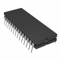
AD7878SQ Analog Devices Inc, AD7878SQ Datasheet - Page 7

AD7878SQ
Manufacturer Part Number
AD7878SQ
Description
IC ADC 12BIT W/DSP INT 28-CDIP
Manufacturer
Analog Devices Inc
Datasheet
1.AD7878JPZ-REEL.pdf
(16 pages)
Specifications of AD7878SQ
Rohs Status
RoHS non-compliant
Number Of Bits
12
Sampling Rate (per Second)
100k
Data Interface
DSP
Number Of Converters
1
Power Dissipation (max)
95.5mW
Voltage Supply Source
Analog and Digital, Dual ±
Operating Temperature
-55°C ~ 125°C
Mounting Type
Through Hole
Package / Case
28-CDIP (0.600", 15.24mm)
Available stocks
Company
Part Number
Manufacturer
Quantity
Price
Part Number:
AD7878SQ
Manufacturer:
ADI/亚德诺
Quantity:
20 000
17 (16 read plus 1 write) operations all occur during t
periods, the conversion time will slip by 17 CLK IN cycles.
Therefore, if read or write operations can occur during t
periods, it means that the conversion time for the ADC can vary
from 7 s to 9.12 s (assuming 8 MHz CLK IN). This calcula-
tion assumes there is a slippage of one CLK IN cycle for each
read or write operation.
INITIATING A CONVERSION
Conversion is initiated on the AD7878 by asserting the CONVST
input. This CONVST input is an asynchronous input indepen-
dent of either the ADC or DSP clocks. This is essential for applica-
tions where precise sampling in time is important. In these applica-
tions the signal sampling must occur at exactly equal intervals to
minimize errors due to sampling uncertainty or jitter. In these cases
the CONVST input is driven from a tamer or some precise clock
source. On receipt of a CONVST pulse, the AD7878 acknowl-
edges by taking the BUSY output low. This BUSY output can be
used to ensure no bus activity while the track/hold goes from track
to hold mode (see Extended Read/Write section). The CONVST
input must stay low for at least two CLK IN periods. The track/
hold amplifier switches from the track to hold mode on the rising
edge of CONVST and conversion is also initiated at this point.
The BUSY output returns high after the CONVST input goes high
and the ADC begins its successive approximation routine. Once
conversion has been initiated another conversion start should not
be attempted until the full conversion cycle has been completed.
Figure 5 shows the taming diagram for the conversion start.
In applications where precise sampling is not critical, the
CONVST pulse can be generated from a microprocessor WR
or RD line gated with a decoded address (different from the
AD7878 CS address). Note that the CONVST pulse width
must be a minimum of two AD7878 CLK IN cycles.
READ/WRITE OPERATIONS
The AD7878 read/write operations consist of reading from the
FIFO memory and reading and writing from the status/control
register. These operations are controlled by the CS, DMRD,
DMWR and ADD0 logic inputs. A description of these operations
is given in the following sections. In addition to the basic read/write
operations there is an extended read/write operation. This can
occur if a read/write operation occurs during a CONVST pulse.
This extended read/write is intended for use with microproces-
sors that can be driven into a WAIT state, and the scheme is
recommended for applications where an external timer controls
the CONVST input asynchronously to the microprocessor read/
write operations.
Basic Read Operation
Figure 6 shows the timing diagram for a basic read operation on
the AD7878. CS and DMRD going low accesses data from
either the status/control register or the FIFO memory. A read
REV. A
Figure 5. Conversion Start Timing Diagram
LOW
LOW
time
–7–
operation with ADD0 low accesses data from the FIFO while a
read with ADD0 high accesses data from the status/ control
register.
Basic Write Operation
A basic write operation to the AD7878 status/control register
consists of bringing CS and DMWR low with ADD0 high. In-
ternally these signals are gated with CLK IN to provide an
internal REGISTER ENABLE signal (see Figure 7). The pulse
width of this REGISTER ENABLE signal is effectively the
overlap between the CLK IN low time and the DMWR pulse.
This may result in shorter write pulse widths, data setup times
and data hold times than those given by the microprocessor.
The timing on the AD7878 timing diagram of Figure 8 is there-
fore given with respect to the internal REGISTER ENABLE
signal rather than the DMWR signal.
Figure 8. Basic Write Operation
Figure 6. Basic Read Operation
Figure 7. DMWR Internal Logic
AD7878


