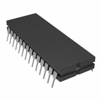
AD7878SQ Analog Devices Inc, AD7878SQ Datasheet - Page 13

AD7878SQ
Manufacturer Part Number
AD7878SQ
Description
IC ADC 12BIT W/DSP INT 28-CDIP
Manufacturer
Analog Devices Inc
Datasheet
1.AD7878JPZ-REEL.pdf
(16 pages)
Specifications of AD7878SQ
Rohs Status
RoHS non-compliant
Number Of Bits
12
Sampling Rate (per Second)
100k
Data Interface
DSP
Number Of Converters
1
Power Dissipation (max)
95.5mW
Voltage Supply Source
Analog and Digital, Dual ±
Operating Temperature
-55°C ~ 125°C
Mounting Type
Through Hole
Package / Case
28-CDIP (0.600", 15.24mm)
Available stocks
Company
Part Number
Manufacturer
Quantity
Price
Part Number:
AD7878SQ
Manufacturer:
ADI/亚德诺
Quantity:
20 000
Establish a single point analog ground (star ground) separate
from the logic system ground at Pin 22 (AGND) or as dose as
possible to the AD7878, as shown in Figure 22. Connect all
other grounds and Pin 7 (AD7878 DGND) to this single analog
ground point. Do not connect any other digital grounds to this
analog ground point. Low impedance analog and digital power
supply common returns are essential to low noise operation of
the ADC, so make the foil width for these tracks as wide as
possible. The use of ground planes minimizes impedance paths
and also guards the analog circuitry from digital noise. The
circuit layouts of Figures 25 and 26 have both analog and digital
ground planes, which are kept separated and only joined to-
gether at the AD7878 AGND pin.
NOISE
Keep the input signal leads to V
AGND (Pin 22) as short as possible to minimize input noise
coupling. In applications where this is not possible, use a
shielded cable between the source and the ADC. Reduce the
ground circuit impedance as much as possible since any poten-
tial difference in grounds between the signal source and the
ADC appears as an error voltage in series with the input signal.
DATA ACQUISITION BOARD
Figure 23 shows the AD7878 in a data acquisition circuit that
will interface directly to either the ADSP-2100, TMS32010 or
the TMS32020. The corresponding printed circuit board (PCB)
layout and silkscreen are shown in Figures 24 to 26.
The only additional component required for a full data acquisi-
tion system is an antialiasing filter. There is a component grid
provided near the analog input on the PCB which may be used
for such a filter or any other conditioning circuitry. To facilitate
this option, a wire link (labelled LK1 on the PCB) is required
on the analog input track. This link connects the input signal to
either the component grid or directly to the buffer amplifier
driving the AD7878 analog input.
Microprocessor connections to the PCB can be made by either
of two ways:
1. 96-contact (3 ROW) Eurocard connector.
2. 26-contact (2 ROW) IDC connector.
The 96-contact Eurocard connector is directly compatible with
the ADSP-2100 Evaluation Board Prototype Expansion Con-
nector. The expansion connector on the ADSP-2100 has eight
decoded drip enable outputs labelled ECE8 to ECE1. ECE6 is
used to drive the AD7878 CS input on the data acquisition
board. To avoid selecting onboard RAM sockets at the same
time, LK6 on the ADSP-2100 board must be removed. In addi-
tion, the expansion connector on the ADSP-2100 has four inter-
REV. A
Figure 22. Power Supply Grounding Practice
IN
and signal return leads from
–13–
rupts labelled EIRQ3 to EIRQ0. The AD7878 ALFL output
connects to EIRQ0. The AD7878 and ADSP-2100 data lines
are aligned for left justified data transfer.
The 26-way IDC connector contains all the necessary contacts
for both the TMS32010 and TMS32020. There are two
switches on the data acquisition board that must be set to en-
able the appropriate interface configuration (see Table III). The
interface connections for the TMS32010/32020 and IDC signal
contact numbers are shown in Table IV and Figure 23. Note the
AD7878 CS input must be decoded from the address bus prior
to the AD7878 evaluation board for the TMS320XX interfaces.
Connections to the analog input (V
are made via two BNC sockets labelled SKT1 and SKT2 on the
silkscreen. If the CONVST input is derived from either the
microprocessor or ADC clock, the effects of clock noise cou-
pling will be reduced.
POWER SUPPLY CONNECTIONS
The PCB requires two analog supplies and one 5 V digital sup-
ply. Connections to the analog supplies are made directly to the
PCB as shown on the silk screen in Figure 24. The connections
are labelled V+ and V– and the range for both of these supplies
is 12 V to 15 V. Connection to the 5 V digital supply is made
through either of the two microprocessor connectors. The +5 V
and –5 V analog power supplies required by the AD7878 are
generated from two voltage regulators on the V+ and V– power
supply inputs (IC3 and IC4 in Figure 23).
IC1
IC2
IC3
IC4
IC5*
IC6*
IC7
SW1
SW2
LK1
C1, C3, C5, C7, C9
C11, C13, C15
C2, C4, C6, C8, C10
C12, C14, C16
R1*, R2*
SKT1, SKT2
SKT3
SKT4
*Not required for ADSP-2100 Interface.
Microprocessor
ADSP-2100
TMS32010
TMS32020
Table III. AD7878 PCB Switch Settings
SWITCH SETTING
COMPONENT LIST
AD711 Op Amp
AD7878 Analog-to-Digital
MC78L05 5 V Regulator
MC79L05 –5 V Regulator
74HC00 Quad NAND Gate
74HC04 Hex Inverter
74HC02 Quad NOR Gate
Single Pole Double Throw
Double Pole Double Throw
Wire Link for Analog Input
10 F Capacitors
0.1 F Capacitors
10 k Resistors
BNC Sockets
26-Contact (2 Row) IDC
96-Contact (3 Row) Eurocard
Converter
Connector
Connector
IN
SW1
A
B
B
) and the CONVST input
AD7878
SW2
A
A
B


