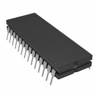
AD7878SQ Analog Devices Inc, AD7878SQ Datasheet - Page 12

AD7878SQ
Manufacturer Part Number
AD7878SQ
Description
IC ADC 12BIT W/DSP INT 28-CDIP
Manufacturer
Analog Devices Inc
Datasheet
1.AD7878JPZ-REEL.pdf
(16 pages)
Specifications of AD7878SQ
Rohs Status
RoHS non-compliant
Number Of Bits
12
Sampling Rate (per Second)
100k
Data Interface
DSP
Number Of Converters
1
Power Dissipation (max)
95.5mW
Voltage Supply Source
Analog and Digital, Dual ±
Operating Temperature
-55°C ~ 125°C
Mounting Type
Through Hole
Package / Case
28-CDIP (0.600", 15.24mm)
Available stocks
Company
Part Number
Manufacturer
Quantity
Price
Part Number:
AD7878SQ
Manufacturer:
ADI/亚德诺
Quantity:
20 000
AD7878
The MC68000 AS and R/W outputs are used to generate sepa-
rate DMWR and DMRD inputs for the AD7878. As with the
three interfaces previously described, WAIT states are inserted if
a read/write operation is attempted while the track/hold amplifier
is going from the track to the hold mode.
Typical AD7878 Microprocessor Operating Sequence
After power-up or reset, the status/control register is initialized
by writing to the AD7878. This enables the ALFL output if
required for a microprocessor interrupt and sets the effective word
length of the FIFO memory. The processor now executes the
main body of the program while waiting for an ADC interrupt.
This interrupt will occur when the preprogrammed number of
samples are collected in the FIFO memory. The interrupt ser-
vice routine first interrogates DB5(FOOR) of the status/control
register to determine if any sample in the FIFO memory is out
of range. If all data samples are valid, then the program pro-
ceeds to read the FIFO memory. If, on the other hand, at least
one sample is out of range, then an overrange routine is called.
There are many actions that can be taken by the out of range
routine, the selection of which is application dependent. One
option is to ignore all the current samples residing in the FIFO
memory, reinitialize the status/control register and return to the
main body of the program. Another option is to check the indi-
vidual out of range status of each word in the FIFO memory
and to discard the invalid ones. The underrange or overrange
status of each word can also be determined and the analog input
adjusted accordingly before returning to the main program.
Note: there is no need to check the out-of-range status if the
analog input is always assured to be within range.
Figure 21. AD7878–MC68000 Interface
–12–
THROUGHPUT RATE
The AD7878 has a maximum specified throughput rate (sample
rate) of 100 kHz. This is a worst-case test condition and specifi-
cations apply for reduced sampling rates, provided that Nyquist
criterion is obeyed. The throughput rate must take into account
ADC CONVST pulse width, ADC conversion time and the
track/hold amplifier acquisition time. The time required for each
of these tasks is shown in Table II for a selection of DSP proces-
sors. Since the ADC clock has to be synchronized to the micro-
processor dock, the conversion time depends on the micro-
processor used. In addition, time must be allowed for reading data
from the AD7878. If this task is performed during the track/
hold amplifier acquisition period, then it does not impact the
overall throughput rate. However, if the read operations occur
during a conversion, they may stretch the conversion time and
reduce the track/hold amplifier acquisition time. The track/hold
amplifier requires a minimum of 2 s to operate to specification.
The time required to read from the AD7878 depends on the
number of FIFO memory locations to be read and the software
organization.
As an example, consider an application using the ADSP-2100
and the AD7878 with a throughput rate of 100 kHz. The time
required for the CONVST pulse and the ADC conversion is
7.375 s. This leaves 2.625 s for the track/hold acquisition
time and for reading the ADC (both operations occurring in
parallel). The ADSP-2100, when operating from a 32 MHz
clock, has an instruction cycle of 125 ns and an interrupt re-
sponse time of 500 ns. This allows adequate time to perform
16 read operations within the time budget allowed.
Number of
Clock Cycles 2 min
ADSP-2100
TMS32010
TMS32020
NOTES
1
2
APPLICATION HINTS
Good printed circuit board (PCB) layout is as important as the
overall circuit design itself in achieving high speed A/D perfor-
mance. The AD7878 is required to make bit decisions on an
LSB size of 1.465 mV. To achieve this, the designer has to be
conscious of noise both in the ADC itself and in the preceding
analog circuitry. Switching mode power supplies are not recom-
mended as the switching spikes will feed through to the com-
parator, causing noisy code transitions. Other concerns are
ground loops and digital feedthrough from microprocessors.
These factors influence any ADC, and a proper PCB layout that
minimizes these effects is essential for best performance.
LAYOUT HINTS
Ensure that the layout for the printed circuit board has the
digital and analog signal lines separated as much as possible.
Take care not to run any digital track alongside an analog signal
track. Guard (screen) the analog input with AGND.
ADSP-2100 Clock Frequency = 32 MHz.
TMS320XX Clock Frequency = 20 MHz.
2
2
1
Table II. AD7878 Throughput Rate
CONVST
Pulse Width Time
250 ns min
400 ns min
400 ns min
Conversion
57 max
7.125 s max 2 s min
11.14 s max 2 s min
11.14 s max 2 s min
T/H Acquisition
Time
Non-
Applicable
REV. A


