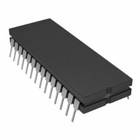
AD7878SQ Analog Devices Inc, AD7878SQ Datasheet - Page 2

AD7878SQ
Manufacturer Part Number
AD7878SQ
Description
IC ADC 12BIT W/DSP INT 28-CDIP
Manufacturer
Analog Devices Inc
Datasheet
1.AD7878JPZ-REEL.pdf
(16 pages)
Specifications of AD7878SQ
Rohs Status
RoHS non-compliant
Number Of Bits
12
Sampling Rate (per Second)
100k
Data Interface
DSP
Number Of Converters
1
Power Dissipation (max)
95.5mW
Voltage Supply Source
Analog and Digital, Dual ±
Operating Temperature
-55°C ~ 125°C
Mounting Type
Through Hole
Package / Case
28-CDIP (0.600", 15.24mm)
Available stocks
Company
Part Number
Manufacturer
Quantity
Price
Part Number:
AD7878SQ
Manufacturer:
ADI/亚德诺
Quantity:
20 000
AD7878–SPECIFICATIONS
Parameter
DYNAMIC PERFORMANCE
DC ACCURACY
ANALOG INPUT
REFERENCE OUTPUT
LOGIC INPUTS
LOGIC OUTPUTS
CONVERSION TIME
POWER REQUIREMENTS
NOTES
1
2
3
4
5
6
Specifications subject to change without notice.
Temperature range as follows: J, K, L versions: 0 C to +70 C; A, B versions: –25 C to +85 C; S version: –55 C to +125 C.
V
SNR calculation includes distortion and noise components.
Measured with respect to the Internal Reference.
For capacitive loads greater than 50 pF a series resistor is required (see Internal Reference section).
Sample tested @ +25 C to ensure compliance.
IN
Signal-to-Noise Ratio (SNR)
T
Total Harmonic Distortion (THD)
Peak Harmonic or Spurious Noise
Intermodulation Distortion (IMD)
Second Order Terms
Third Order Terms
Track/Hold Acquisition Time
Resolution
Minimum Resolution for Which
Relative Accuracy
Differential Nonlinearity
Bipolar Zero Error
Positive Full-Scale Error
Negative Full-Scale Error
Input Voltage Range
Input Current
REF OUT
REF OUT Error @ 25 C
T
Reference Load Sensitivity
Input High Voltage, V
Input Low Voltage, V
Input Current, I
Input Capacitance, C
Output High Voltage, V
Output Low Voltage, V
DB11–DB0
V
V
V
I
I
I
Power Dissipation
DD
CC
SS
= 3 V. See Dynamic Specifications section.
MIN
MIN
DD
CC
SS
No Missing Codes are Guaranteed
( REF OUT/ I)
Floating State Leakage Current
Floating State Output Capacitance
to T
to T
MAX
MAX
IN
IN
INL
INH
5
6
OL
OH
4
4
2
3
@ 25 C
6
J, A
Versions
70
70
–80
–80
–80
–80
2
12
12
3
+2.4
+0.8
10
+2.7
+0.4
15
7/7.125
7/9.250
+5
+5
–5
13
100
6
95.5
1/2
1/2
6
6
6
3
550
10
15
1
10
10
1
K, L, B
Versions Version
72
71
–80
–80
–80
–80
2
12
12
3
+2.4
+0.8
10
+2.7
+0.4
15
7/7.125
7/9.250
+5
+5
–5
13
100
6
95.5
1/4
1/2
6
6
6
3
550
10
15
1
10
10
(V
0 V, f
DD
= +5 V
CLK
= 8 MHz. All Specifications T
S
70
70
–78
–78
–78
–78
2
12
12
3
+2.4
+0.8
10
+2.7
+0.4
15
7/7.125
7/9.250
+5
+5
–5
13
100
6
95.5
1/2
1/2
6
6
6
3
550
10
15
1
10
10
–2–
5%, V
Units
dB min
dB min
dB max
dB max
dB max
dB max
Bits
Bits
LSB typ
LSB typ
LSB max
LSB max
LSB max
Volts
V nom
mV max
mV max
mV max
V min
V max
pF max
V min
V max
15
V nom
V nom
V nom
mA max
mA max
mW max
s max
A max
A max
s min/ s max
s min/ s max
A max
CC
10
= +5 V
5%, V
MIN
Test Conditions/Comments
V
Typically 71.5 dB for 0 < V
V
Typically –86 dB for 0 < V
V
Typically –86 dB for 0 < V
fa = 9 kHz, fb = 9.5 kHz, f
fa = 9 kHz, fb = 9.5 kHz, f
See Throughput Rate Section
Reference Load Current Change (0 A–500 A).
Reference Load Should Not Be Changed
During Conversion
V
V
V
I
I
pF max
Assuming No External Read/Write Operations
Assuming 17 External Read/Write Operations
See Internal Comparator Timing Section
CS = DMWR = DMRD = 5 V
CS = DMWR = DMRD = 5 V
CS = DMWR = DMRD = 5 V
Typically 60 mW
SOURCE
SINK
A max
5% for Specified Performance
5% for Specified Performance
5% for Specified Performance
IN
IN
IN
CC
CC
IN
SS
to T
= 10 kHz Sine Wave, f
= 10 kHz Sine Wave, f
= 10 kHz, f
= 0 to V
= +5 V
= +5 V
= –5 V
= 1.6 mA
MAX
40 A
, unless otherwise noted.)
CC
5%
5%
5%, AGND = DGND =
SAMPLE
= 100 kHz
SAMPLE
SAMPLE
SAMPLE
SAMPLE
IN
IN
IN
< 50 kHz
< 50 kHz
< 50 kHz
= 100 kHz
= 100 kHz
= 50 kHz
= 50 kHz
REV. A


