AD7878SQ Analog Devices Inc, AD7878SQ Datasheet - Page 4
AD7878SQ
Manufacturer Part Number
AD7878SQ
Description
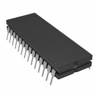
IC ADC 12BIT W/DSP INT 28-CDIP
Manufacturer
Analog Devices Inc
Datasheet
1.AD7878JPZ-REEL.pdf
(16 pages)
Specifications of AD7878SQ
Rohs Status
RoHS non-compliant
Number Of Bits
12
Sampling Rate (per Second)
100k
Data Interface
DSP
Number Of Converters
1
Power Dissipation (max)
95.5mW
Voltage Supply Source
Analog and Digital, Dual ±
Operating Temperature
-55°C ~ 125°C
Mounting Type
Through Hole
Package / Case
28-CDIP (0.600", 15.24mm)
Available stocks
Company
Part Number
Manufacturer
Quantity
Price

Part Number:
AD7878SQ
Manufacturer:
ADI/亚德诺
Quantity:
20 000


AD7878
Pin
Number
11
12
13
14
15
16
17
18
19
10–15
16–19
20
21
22
23
24
25
26
27
28
Mnemonic
ADD0
CS
DMWR
DMRD
BUSY
ALFL
DGND
V
DB11
DB10–DB5
DB4–DB1
DB0
V
AGND
REF OUT
V
V
CONVST
RESET
CLK IN
Pin
CC
DD
IN
SS
DIP
Function
Address Input. This control input determines whether the word placed on the output data bus during a read operation is a data
word from the FIFO RAM or the contents of the status/control register. A logic low accesses the data word from Location 0 of
the FIFO while a logic high selects the contents of the register (see Status/Control Register section).
Chip Select. Active low logic input. The device is selected when this input is active.
Dam Memory Write. Active low logic input. DMWR is used in conjunction with CS low and ADD0 high to write data to the
status/control register. Corresponds to DMWR (ADSP-2100), R/W (MC68000, TMS32020), WE (TMS32010).
Data Memory READ. Active low logic input. DMRD is used in conjunction with CS low to enable the three-state output buffers.
Corresponds directly to DMRD (ADSP-2100), DEN (TMS32010).
Active Low Logic Output. This output goes low when the ADC receives a CONVST pulse and remains low until the track/hold
has gone into its hold mode. The three-state drivers of the AD7878 can be disabled while the BUSY signal is low (see Extended
READ/WRITE section). This is achieved by writing a logic 0 to DB5 (DISO) of the status/control register. Writing a logic 1 to
DB5 of the status/control register allows data to be accessed from the AD7878 while BUSY is low.
FIFO Almost Full. A logic low indicates that the word count (i.e., number of conversion results) in the FIFO memory has
reached the programmed word count in the status/control register. ALFL is updated at the end of each conversion. The ALFL
output is reset to a logic high when a word is read from the FIFO memory and the word count is less than the preprogrammed
word count. It can also be set high by writing a logic 1 to DB7 (ENAF) of the status/control register.
Digital Ground. Ground reference for digital circuitry.
Digital supply voltage, +5 V
Data Bit 11 (MSB). Three-state TTL output. Coding for the data words in FIFO RAM is twos complement.
Data Bit 10 to Data Bit 5. Three-state TTL input/outputs.
Data Bit 4 to Data Bit 1. Three-state TTL outputs.
Data Bit 0 (LSB). Three-state TTL output.
Analog positive supply voltage, +5 V
Analog Ground. Ground reference for track/hold, reference and DAC.
Voltage Reference Output. The internal 3 V analog reference is provided at this pin. The external load capability of the reference
is 500 A.
Analog Input. Analog input range is 3 V.
Analog negative supply voltage, –5 V
Convert Start. Logic input. A low to high transition on this input puts the track/hold into its hold mode and starts conversion.
The CONVST input is asynchronous to CLK IN and independent of CS, DMWR and DMRD.
Reset. Active low logic input. A logic low sets the words in FIFO memory to 1000 0000 0000 and resets the ALFL output and
status/control register.
Clock Input. TTL-compatible logic input. Used as the clock source for the A/D converter. The mark-space ratio of this clock can
vary from 35/65 to 65/35.
5%. Positive supply voltage for digital circuitry.
PIN FUNCTION DESCRIPTION
PIN CONFIGURATIONS
5%.
5%.
PLCC
–4–
LCCC
REV. A
Related parts for AD7878SQ
Image
Part Number
Description
Manufacturer
Datasheet
Request
R

Part Number:
Description:
±1.7g Dual-Axis IMEMS Accelerometer Evaluation Board
Manufacturer:
Analog Devices Inc
Datasheet:

Part Number:
Description:
Inertial Sensor Evaluation System
Manufacturer:
Analog Devices Inc
Datasheet:
Part Number:
Description:
Manufacturer:
Analog Devices Inc
Datasheet:
Part Number:
Description:
Manufacturer:
Analog Devices Inc
Datasheet:
Part Number:
Description:
Manufacturer:
Analog Devices Inc
Datasheet:
Part Number:
Description:
Manufacturer:
Analog Devices Inc
Datasheet:
Part Number:
Description:
Manufacturer:
Analog Devices Inc
Datasheet:
Part Number:
Description:
Manufacturer:
Analog Devices Inc
Datasheet:
Part Number:
Description:
Manufacturer:
Analog Devices Inc
Datasheet:
Part Number:
Description:
Manufacturer:
Analog Devices Inc
Datasheet:
Part Number:
Description:
Manufacturer:
Analog Devices Inc
Datasheet:
Part Number:
Description:
Manufacturer:
Analog Devices Inc
Datasheet:
Part Number:
Description:
Manufacturer:
Analog Devices Inc
Datasheet: