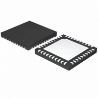
MAX1358BETL+ Maxim Integrated Products, MAX1358BETL+ Datasheet - Page 27

MAX1358BETL+
Manufacturer Part Number
MAX1358BETL+
Description
IC DAS 16BIT 40-TQFN
Manufacturer
Maxim Integrated Products
Type
Data Acquisition System (DAS)r
Datasheet
1.MAX1358BETL.pdf
(71 pages)
Specifications of MAX1358BETL+
Resolution (bits)
16 b
Sampling Rate (per Second)
21.84k
Data Interface
Serial
Voltage Supply Source
Analog and Digital
Voltage - Supply
1.8 V ~ 3.6 V
Operating Temperature
-40°C ~ 85°C
Mounting Type
Surface Mount
Package / Case
40-TQFN Exposed Pad
Number Of Converters
2
Resolution
16 bit
Interface Type
Serial (4-Wire, SPI, QSPI, Microwire)
Voltage Reference
1.25 V
Supply Voltage (max)
3.6 V
Supply Voltage (min)
1.8 V
Maximum Power Dissipation
2051.3 mW
Maximum Operating Temperature
+ 85 C
Mounting Style
SMD/SMT
Input Voltage
1.8 V to 3.6 V
Minimum Operating Temperature
- 40 C
Lead Free Status / RoHS Status
Lead free / RoHS Compliant
16-Bit, Data-Acquisition System with ADC, DACs,
and dynamic range constraints. The force-sense DAC
provides 10-bit resolution for precise sensor applica-
tions. The ADC and DACs both utilize a low-drift 1.25V
internal bandgap reference for conversions and full-
scale range setting. The RTC has a 138-year range and
provides an alarm function that can be used to wake up
the system or cause an interrupt at a predefined time.
The power-supply voltage monitor detects when DV
falls below a trip threshold voltage of +1.8V and asserts
RESET. The MAX1358B uses a 4-wire serial interface to
communicate directly among SPI, QSPI, or
MICROWIRE devices for system configuration and
readback functions.
The MAX1358B includes a sigma-delta ADC with pro-
grammable conversion rate, a PGA, and a dual 10:1
input mux. When performing continuous conversions at
10sps or single conversions at the 40sps setting (effec-
tively 10sps due to four sample sigma-delta settling),
the ADC has 16-bit noise-free resolution. The noise-free
resolution drops to 10 bits at the maximum sampling
rate of 477sps. Differential inputs support unipolar
(between 0 and V
modes of operation. Note: Avoid combinations of input
signal and PGA gains that exceed the reference range
at the ADC input. The ADOU bit in the STATUS register
indicates if the ADC has overranged or underranged.
Zero-scale and full-scale calibrations remove offset and
gain errors. Direct access to gain and zero-scale cali-
bration registers allows system-level offset and gain cal-
ibration. The zero-scale adjustment register allows
intentional positive offset skewing to preserve unipolar-
mode resolution for signals that have a slight negative
offset (i.e., unipolar clipping near zero can be removed).
Perform ADC calibration whenever the ADC configura-
tion, temperature, or AV
tus can be programmed to provide an interrupt on INT
or on any UPIO_.
An integrated PGA provides four selectable gains (+1V/V,
+2V/V, +4V/V, and +8V/V) to maximize the dynamic
range of the ADC. Bits GAIN1 and GAIN0 set the gain
(see the ADC Register for more information). The PGA
gain is implemented in the digital filter of the ADC.
UPIOs, RTC, Voltage Monitors, and Temp Sensor
Analog-to-Digital Converter (ADC)
______________________________________________________________________________________
REF
) and bipolar (between ±V
DD
changes. The ADC-done sta-
PGA Gain
REF
DD
)
The MAX1358B performs analog-to-digital conversions
using a single-bit, 3rd-order, switched-capacitor sigma-
delta modulator. The sigma-delta modulation converts
the input signal into a digital pulse train whose average
duty cycle represents the digitized signal information.
The pulse train is then processed by a digital decimation
filter. The modulator provides 2nd-order frequency shap-
ing of the quantization noise resulting from the single-bit
quantizer. The modulator is fully differential for maximum
signal-to-noise ratio and minimum susceptibility to
power-supply noise.
INT asserts (and remains asserted) within 30µs when
the differential voltage on the selected analog inputs
exceeds the signal-detect comparator trip threshold.
The signal-detect comparator’s differential input trip
threshold (i.e., offset) is user selectable and can be pro-
grammed to the following values: 0mV, 50mV, 100mV,
150mV, or 200mV.
The ADC provides two external analog inputs: AIN1
and AIN2. The rail-to-rail inputs accept differential or
single-ended voltages, or external temperature-sensing
diodes. The unused op amps, switches, or DAC inputs
and output pins can also be used as rail-to-rail analog
inputs if the associated function is disabled.
Internal protection diodes clamp the analog inputs to
AV
from (AGND - 0.3V) to (AV
conversions near full scale, the inputs must not exceed
AV
50mV. If the inputs exceed (AGND - 0.3V) to (AV
0.3V), limit the current to 50mA.
The MAX1358B includes a dual 10:1 mux for the positive
and negative inputs of the ADC. Figure 3 illustrates which
signals are present at the inputs of each mux for the
MAX1358B. The MUXP[3:0] and MUXN[3:0] bits of the
MUX register select the input to the ADC and the signal-
detect comparator (Tables 8 and 9). See the MUX register
description in the Register Definitions section for multi-
plexer functionality. The POL bit of the ADC register
swaps the polarity of mux output signals to the ADC.
DD
DD
and AGND and allow the channel input to swing
by more than 50mV or be lower than AGND by
Signal-Detect Comparator
DD
Analog Input Protection
+ 0.3V). For accurate
Analog Inputs
ADC Modulator
Analog Mux
DD
27
+


