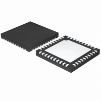
MAX1358BETL+ Maxim Integrated Products, MAX1358BETL+ Datasheet - Page 7

MAX1358BETL+
Manufacturer Part Number
MAX1358BETL+
Description
IC DAS 16BIT 40-TQFN
Manufacturer
Maxim Integrated Products
Type
Data Acquisition System (DAS)r
Datasheet
1.MAX1358BETL.pdf
(71 pages)
Specifications of MAX1358BETL+
Resolution (bits)
16 b
Sampling Rate (per Second)
21.84k
Data Interface
Serial
Voltage Supply Source
Analog and Digital
Voltage - Supply
1.8 V ~ 3.6 V
Operating Temperature
-40°C ~ 85°C
Mounting Type
Surface Mount
Package / Case
40-TQFN Exposed Pad
Number Of Converters
2
Resolution
16 bit
Interface Type
Serial (4-Wire, SPI, QSPI, Microwire)
Voltage Reference
1.25 V
Supply Voltage (max)
3.6 V
Supply Voltage (min)
1.8 V
Maximum Power Dissipation
2051.3 mW
Maximum Operating Temperature
+ 85 C
Mounting Style
SMD/SMT
Input Voltage
1.8 V to 3.6 V
Minimum Operating Temperature
- 40 C
Lead Free Status / RoHS Status
Lead free / RoHS Compliant
ELECTRICAL CHARACTERISTICS (continued)
(AV
10µF, 10µF between CF+ and CF-, T
16-Bit, Data-Acquisition System with ADC, DACs,
Input Capacitance
CHARGE PUMP
Maximum Output Current
Output Voltage
Output-Voltage Ripple
Load Regulation
REG Input Voltage Range
REG Input Current
CPOUT Input Voltage Range
CPOUT Input Leakage Current
SIGNAL-DETECT COMPARATOR
Differential Input-Detection
Threshold Voltage
Differential Input-Detection
Threshold Error
Common-Mode Input Voltage
Range
Turn-On Time
VOLTAGE MONITORS
DV
Range
Trip Threshold (DV
DV
Period
DV
UPIOs, RTC, Voltage Monitors, and Temp Sensor
DD
DD
DD
DD
= DV
Monitor Supply Voltage
Monitor Timeout Reset
Monitor Hysteresis
PARAMETER
DD
= +1.8V to +3.6V, V
DD
_______________________________________________________________________________________
Falling)
A
REF
= T
SYMBOL
I
= +1.25V, external reference, f
MIN
OUT
to T
MAX
SNO_, SNC_, or SCM_ = AV
switch connected to enabled mux input
No load
I
I
capacitor (Note 2)
I
capacitor
Internal linear regulator disabled (Note 2)
Linear regulator off, charge pump off
Charge pump disabled
Charge pump disabled
TSEL[2:0] = 0 hex
TSEL[2:0] = 4 hex
TSEL[2:0] = 5 hex
TSEL[2:0] = 6 hex
TSEL[2:0] = 7 hex
For valid reset (Note 7)
HYSE bit set to logic 1
HYSE bit set to logic 0
OUT
OUT
OUT
, unless otherwise noted. Typical values are at T
= 10mA
= 10mA, excluding ESR of external
= 10mA, excluding ESR of external
CONDITIONS
CLK32K
DD
= 32.768kHz (external clock), C
or AGND;
V
MIN
AGND
1.80
A
3.2
3.0
1.6
1.8
1.4
10
= +25°C.) (Note 1)
TYP
1.85
100
150
200
±10
225
2.5
3.3
1.5
15
50
45
40
3
2
0
REG
= 10µF, C
AV
MAX
1.95
3.6
1.8
3.6
3.6
50
20
DD
CPOUT
mV/mA
UNITS
mV
mA
mV
mV
mV
pF
nA
nA
µs
V
V
V
V
V
V
s
P-P
7
=


