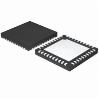
MAX1358BETL+ Maxim Integrated Products, MAX1358BETL+ Datasheet - Page 58

MAX1358BETL+
Manufacturer Part Number
MAX1358BETL+
Description
IC DAS 16BIT 40-TQFN
Manufacturer
Maxim Integrated Products
Type
Data Acquisition System (DAS)r
Datasheet
1.MAX1358BETL.pdf
(71 pages)
Specifications of MAX1358BETL+
Resolution (bits)
16 b
Sampling Rate (per Second)
21.84k
Data Interface
Serial
Voltage Supply Source
Analog and Digital
Voltage - Supply
1.8 V ~ 3.6 V
Operating Temperature
-40°C ~ 85°C
Mounting Type
Surface Mount
Package / Case
40-TQFN Exposed Pad
Number Of Converters
2
Resolution
16 bit
Interface Type
Serial (4-Wire, SPI, QSPI, Microwire)
Voltage Reference
1.25 V
Supply Voltage (max)
3.6 V
Supply Voltage (min)
1.8 V
Maximum Power Dissipation
2051.3 mW
Maximum Operating Temperature
+ 85 C
Mounting Style
SMD/SMT
Input Voltage
1.8 V to 3.6 V
Minimum Operating Temperature
- 40 C
Lead Free Status / RoHS Status
Lead free / RoHS Compliant
hysteresis helps eliminate chatter when running directly off
unregulated batteries. If DV
power-on reset circuitry is enabled and the HYSE bit is
deasserted setting the hysteresis back to +20mV. The
power-on default is 0.
16-Bit, Data-Acquisition System with ADC, DACs,
UPIOs, RTC, Voltage Monitors, and Temp Sensor
The STATUS register contains the status bits of events in
various system blocks. Any status bits not masked in the
IMSK register cause an interrupt on INT. Some of the
status bit setting events (GPI, WAKEUP, ALARM, DRDY)
can be directed to UPIO_ to provide multiple µC inter-
rupt inputs. There are no specific mask bits for the UPIO
interrupt signals since the bits are effectively masked by
selecting a different function for UPIO. The STATUS bits
always record the triggering event(s), even for masked
bits, which do not generate an interrupt on INT. It is pos-
sible to set multiple STATUS bits during a single INT
interrupt event. Clear all STATUS bits except for ADD
and ADOU by reading the STATUS register. During a
STATUS register read, INT deasserts when the first
STATUS data bit (LDVD) reads out (9th rising SCLK) and
remains deasserted until shortly after the last STATUS
data bit (~15ns). At this point, INT reasserts if any
STATUS bit is set during the STATUS register read. If the
STATUS register is partially read (i.e., the read is aborted
midway), none of the STATUS bits are cleared. New
events occurring during a STATUS register read, or
events that persist after reading the STATUS bits result in
another interrupt immediately after the STATUS register
read finishes. This is a read-only register.
LDVD: Low DV
indicates DV
LDVD = 0. LDVD clears during the STATUS register
read as long as the condition does not persist.
Otherwise, the LDVD bit reasserts immediately. If the
DV
power-on default is 0.
LCPD: Low CPOUT voltage-detector status bit. LCPD =
1 indicates CPOUT is below the +2.7V threshold; other-
wise LCPD = 0. LCPD clears during the STATUS regis-
ter read as long as the condition does not persist.
Otherwise the LCPD bit reasserts immediately. LCPD =
0 when the CPOUT low voltage detector is disabled.
The power-on default is 0.
STATUS Register (Power-On State: 0000 000X 0000 0000)
58
DD
______________________________________________________________________________________
LDVD
UPR4
MSB
low voltage detector is disabled, LDVD = 0. The
DD
DD
is below the +1.8V threshold; otherwise
voltage-detector status bit. LDVD = 1
LCPD
UPR3
DD
falls below +1.3V (typ), the
ADOU
UPR2
UPR1
SDC
RSTE: RESET output enable bit. Set RSTE = 1 to
enable RESET to be controlled by the +1.8V DV
supply-voltage detector, and set RSTE = 0 to disable
this control. The power-on default is 1.
ADOU: ADC overflow/underflow status bit. ADOU = 1
indicates an ADC underflow or overflow condition in the
current ADC result. New conversions that are valid
clear the ADOU bit. ADOU = 0 when the ADC data is
valid or the ADC is disabled (ADCE = 0). An underflow
condition occurs when the ADC data is theoretically
less than 0000 hex in unipolar mode and less than
8000 hex in bipolar mode. An overflow condition occurs
when the ADC data is theoretically greater than FFFF
hex in unipolar mode and greater than 7FFF hex in
bipolar mode. Use this bit to determine the validity of
an ADC result at the maximum or minimum code values
(i.e., 0000 hex or FFFF hex for unipolar mode and 8000
hex and 7FFF hex for bipolar mode). The power-on
default is 0. Reading the STATUS register does not
clear the ADOU bit.
SDC: Signal-detect comparator status bit. When
SDC = 1, the positive input to the signal-detect compara-
tor exceeds the negative input plus the programmed
threshold voltage. The SDC bit clears during the STATUS
register read unless the condition remains true. The SDC
bit also deasserts when the signal-detect comparator
powers down (SDCE = 0). The power-on default is 0.
CRDY: High-frequency-clock ready status bit.
CRDY = 1 indicates a locked high-frequency clock to
the 32kHz reference frequency by the FLL. The CRDY
bit clears during the STATUS register read. This bit only
asserts after power-up or after enabling the FLL using
the FLLE bit. The power-on default is 0.
ADD: ADC-done status bit. ADD = 1 indicates a com-
pleted ADC conversion or calibration. Clear the ADD bit
by reading the appropriate ADC data, offset, or gain-cali-
bration registers. The ADC status bit also clears when a
new ADC result updates to the data or calibration regis-
ters (i.e., it follows the assertion level of the UPIO =
DRDY signal). Reading the STATUS register does not
clear this bit. This bit is equivalent to the DRDY signal
available through UPIO_. The power-on default is 0.
CRDY
UPF4
UPF3
ADD
UPF2
ALD
UPF1
LSB
DD
X
low-


