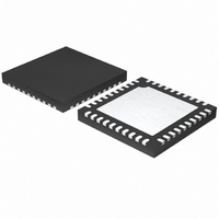
MAX1358BETL+ Maxim Integrated Products, MAX1358BETL+ Datasheet - Page 28

MAX1358BETL+
Manufacturer Part Number
MAX1358BETL+
Description
IC DAS 16BIT 40-TQFN
Manufacturer
Maxim Integrated Products
Type
Data Acquisition System (DAS)r
Datasheet
1.MAX1358BETL.pdf
(71 pages)
Specifications of MAX1358BETL+
Resolution (bits)
16 b
Sampling Rate (per Second)
21.84k
Data Interface
Serial
Voltage Supply Source
Analog and Digital
Voltage - Supply
1.8 V ~ 3.6 V
Operating Temperature
-40°C ~ 85°C
Mounting Type
Surface Mount
Package / Case
40-TQFN Exposed Pad
Number Of Converters
2
Resolution
16 bit
Interface Type
Serial (4-Wire, SPI, QSPI, Microwire)
Voltage Reference
1.25 V
Supply Voltage (max)
3.6 V
Supply Voltage (min)
1.8 V
Maximum Power Dissipation
2051.3 mW
Maximum Operating Temperature
+ 85 C
Mounting Style
SMD/SMT
Input Voltage
1.8 V to 3.6 V
Minimum Operating Temperature
- 40 C
Lead Free Status / RoHS Status
Lead free / RoHS Compliant
The MAX1358B contains an on-chip digital lowpass fil-
ter that processes the data stream from the modulator
using a sinc
settling time of four output data periods (4 x 200ms).
The MAX1358B has 25% overrange capability built into
the modulator and digital filter:
Figure 4 shows the filter frequency response. The sinc
characteristic -3dB cutoff frequency is 0.228 times the
first notch frequency.
The output data rate for the digital filter corresponds
with the positioning of the first notch of the filter’s fre-
quency response. The notches of the sinc
repeated at multiples of the first notch frequency. The
sinc
at these notches. For example, 50Hz is equal to five
times the first notch frequency and 60Hz is equal to six
times the first notch frequency.
16-Bit, Data-Acquisition System with ADC, DACs,
UPIOs, RTC, Voltage Monitors, and Temp Sensor
Figure 4. Filter Frequency Response
28
4
______________________________________________________________________________________
filter provides an attenuation of better than 100dB
-120
-160
-200
-40
-80
4
0
(sinx/x)
0
H f
( ) =
20
4
⎡
⎢
⎢
⎢
⎢
⎢
⎣
N
response. The sinc
1
40
SIN N
FREQUENCY (Hz)
SIN
⎛
⎜
⎝
⎛
⎜
⎝
60
π
π
f
m
f
f
m
f
⎞
⎟
⎠
80
Digital Filtering
⎞
⎟
⎠
⎤
⎥
⎥
⎥
⎥
⎥
⎦
4
100
4
120
filter has a
4
filter are
4
The MAX1358B incorporates two 10-bit force-sensing
DACs. The DACs’ reference voltage sets the full-scale
range. Program the DACA_OP register using the serial
interface to set the output voltages of the DAC at OUTA.
Connecting resistors in a voltage-divider configuration
between OUTA, FBA, and GND sets a different closed-
loop gain for the output amplifier (see the Applications
Information section).
The DAC output amplifier typically settles to ±0.5 LSB
from a full-scale transition within 65µs (unity gain and
loaded with 10kΩ in parallel with 200pF). Loads of less
than 1kΩ could degrade performance. See the Typical
Operating Characteristics for the source-and-sink
capability of the DAC output.
The MAX1358B features a software-programmable
shutdown mode for the DAC. Power down DACA or
DACB independently or simultaneously by clearing the
DAE and DBE bits (see the DACA_OP Register and
DACB_OP Register sections). DAC output OUTA and
OUTB go high impedance when powered down. The
DACs are normally powered down at power-on reset.
The charge pump provides > 3V at CPOUT with a maxi-
mum 10mA load. Enable the charge pump through the
PS_VMONS register. The charge pump is powered
from DV
the charge pump and linear regulator. The charge
pump is disabled at power-on reset.
An internal clock drives the charge-pump clock and
ADC clock. The charge pump delivers a maximum
10mA of current to external devices. The droop and the
ripple depend on the clock frequency (f
32.768kHz/2), switch resistances (R
the external capacitors (10µF) along with their respec-
tive ESRs, as shown below.
R
OUT
V
RIPPLE
=
DD
f
CLK F
. See Figures 5 and 6 for block diagrams of
1
V
C
=
DROOP
f
CLK CPOUT
+
2
I
C
OUT
R
=
SWITCH
I
OUT OUT
R
+
+
2
Force-Sense DAC
4
I
OUT
ESR
SWITCH
ESR
Charge Pump
C
F
C
+
CPOUT
ESR
= 5Ω), and
C
CLK
CPOUT
=


