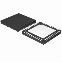
MAX1358BETL+ Maxim Integrated Products, MAX1358BETL+ Datasheet - Page 63

MAX1358BETL+
Manufacturer Part Number
MAX1358BETL+
Description
IC DAS 16BIT 40-TQFN
Manufacturer
Maxim Integrated Products
Type
Data Acquisition System (DAS)r
Datasheet
1.MAX1358BETL.pdf
(71 pages)
Specifications of MAX1358BETL+
Resolution (bits)
16 b
Sampling Rate (per Second)
21.84k
Data Interface
Serial
Voltage Supply Source
Analog and Digital
Voltage - Supply
1.8 V ~ 3.6 V
Operating Temperature
-40°C ~ 85°C
Mounting Type
Surface Mount
Package / Case
40-TQFN Exposed Pad
Number Of Converters
2
Resolution
16 bit
Interface Type
Serial (4-Wire, SPI, QSPI, Microwire)
Voltage Reference
1.25 V
Supply Voltage (max)
3.6 V
Supply Voltage (min)
1.8 V
Maximum Power Dissipation
2051.3 mW
Maximum Operating Temperature
+ 85 C
Mounting Style
SMD/SMT
Input Voltage
1.8 V to 3.6 V
Minimum Operating Temperature
- 40 C
Lead Free Status / RoHS Status
Lead free / RoHS Compliant
A CMOS signal can be used to drive 32KIN if it is divid-
ed down. Figure 25 is an example circuit, which works
well.
The mux inputs can range between AGND and AV
However, when the internal temperature sensor is
enabled, AIN1 and AIN2 cannot exceed 0.7V. This
necessitates additional circuitry to divide down the
input signal. See Figure 26 for an example circuit that
divides down backlight V
AIN1 pin.
Figure 27 illustrates the MAX1358B in a complete opti-
cal reflectometry application with two transmitting LEDs
and one receiving photodiode. The LEDs transmit light
at a specific wavelength onto the sample strip, and the
photodiode receives the reflections from the strip. Set
the DAC to provide appropriate bias currents for the
LEDs. Always keep the photodiodes reverse-biased or
zero-biased. SPDT1 and SPDT2 switch between the
two LEDs.
The MAX1358B family interface with electrochemical
sensors. The 10-bit DAC with the force-sense buffers
have the flexibility to connect to many different types of
sensors. An external precision resistor completes the
transimpedance amplifier configuration to convert the
current generated by the sensor to a voltage measure-
ment using the ADC. The induced error from this source
is negligible due to FBA’s extremely low input bias cur-
rent. Internally, the ADC can differentially measure
directly across the external transimpedance resistor,
RF, eliminating any errors due to voltages drifting over
time, temperature, or supply voltage.
16-Bit, Data-Acquisition System with ADC, DACs,
Figure 25. Clocking with a CMOS Signal
UPIOs, RTC, Voltage Monitors, and Temp Sensor
Optical Reflectometry Application with
CMOS CLOCK
(0 TO DV
Electrochemical Sensor Operation
DD
)
Dual LED and Single Photodiode
Clocking with a CMOS Signal
______________________________________________________________________________________
100kΩ
100kΩ
DD
to work properly with the
Input Multiplexer
32KIN
MAX1358B
DD
.
Use two diode-connected 2N3904 transistors for exter-
nal temperature sensing in Figure 29. Select AIN1 and
AIN2 through the positive and negative mux, respec-
tively. For internal temperature sensor measurements,
set MUXP<3:0> to 0111, and set MUXN<3:0> to 0000.
The analog input signals feed through a PGA to the
ADC for conversion.
The MAX1358B integrated PWM is available for LCD
bias control, sensor-bias voltage trimming, buzzer drive,
and duty-cycled sleep-mode power-control schemes.
Figure 30 shows the MAX1358B performing LCD bias
control. A sensor-bias voltage trimming application is
shown in Figure 31. Figures 33 and 34 show the PWM
circuitry being used in a single-ended and differential
piezoelectric buzzer-driving application.
Internal to the MAX1358B, the ADC is 24 bits and is
always in bipolar mode. The OFFSET CAL and GAIN
CAL data is also 24 bits. The conversion to unipolar and
the gain are performed digitally. The default values for
the OFFSET CAL and GAIN CAL registers in the
MAX1358B are 00 0000h and 80 0000h, respectively.
The calibration works as follows:
where ADC is the conversion result in the DATA register,
RAW is the output of the decimation filter internal to the
MAX1358B, OFFSET is the value stored in the OFFSET
CAL register, Gain is the value stored in the GAIN CAL
register, and PGA is the selected PGA gain found in the
ADC register as GAIN<1:0>. In unipolar mode, all nega-
tive values return a zero result and an additional gain of 2
is added.
Figure 26. Input Multiplexer
V
BATT1
ADC = (RAW - OFFSET) x Gain x PGA
V
MAX1358B
REF
x2
= 1.25V
μP
Temperature Measurement with
UPIO1
V
AIN1
BATT2
GPIOn
BATTVCHECK
Two Remote Sensors
< 0.6125V
ADC Calibration
NOTE:
GPIOn IS LOW = LED ON,
HIGH-Z = LED OFF
BACKLIGHT
V
DD
63


