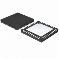
MAX1358BETL+ Maxim Integrated Products, MAX1358BETL+ Datasheet - Page 42

MAX1358BETL+
Manufacturer Part Number
MAX1358BETL+
Description
IC DAS 16BIT 40-TQFN
Manufacturer
Maxim Integrated Products
Type
Data Acquisition System (DAS)r
Datasheet
1.MAX1358BETL.pdf
(71 pages)
Specifications of MAX1358BETL+
Resolution (bits)
16 b
Sampling Rate (per Second)
21.84k
Data Interface
Serial
Voltage Supply Source
Analog and Digital
Voltage - Supply
1.8 V ~ 3.6 V
Operating Temperature
-40°C ~ 85°C
Mounting Type
Surface Mount
Package / Case
40-TQFN Exposed Pad
Number Of Converters
2
Resolution
16 bit
Interface Type
Serial (4-Wire, SPI, QSPI, Microwire)
Voltage Reference
1.25 V
Supply Voltage (max)
3.6 V
Supply Voltage (min)
1.8 V
Maximum Power Dissipation
2051.3 mW
Maximum Operating Temperature
+ 85 C
Mounting Style
SMD/SMT
Input Voltage
1.8 V to 3.6 V
Minimum Operating Temperature
- 40 C
Lead Free Status / RoHS Status
Lead free / RoHS Compliant
The REF_SDC register contains bits to control the refer-
ence voltage and signal-detect comparator.
REFV<1:0>: Reference buffer voltage gain and enable
bits. Enables the output buffer, and sets the gain and
the voltage at the REF pin as shown in Table 10. Power-
on state is off to enable an external reference to drive
the REF pin without contention.
AOFF: ADC and DAC/op-amp power-off bit. This bit pro-
vides a method for turning off several analog functions
with a single write. Setting AOFF = 1 deasserts the
ADCE in the ADC register and the DAE, DBE, and OP1E
bits in the DACA_OP and DACB_OP registers, powering
down these analog blocks. Setting AOFF = 0 has no
effect. The AON bit has priority when both AON and
AOFF bits are asserted.
Most of the analog functions can be disabled with a
single write to the REF_SDC register by using AOFF,
REFV<1:0>, and SDCE.
16-Bit, Data-Acquisition System with ADC, DACs,
UPIOs, RTC, Voltage Monitors, and Temp Sensor
REF_SDC Register (Power-On State: 0000 0000)
Table 10. Setting the Reference Output
Voltage
42
BUFFER GAIN
REFERENCE
REFV1
______________________________________________________________________________________
Disabled
MSB
1.638
(V/V)
1.0
2.0
REFV0
VOLTAGE (V)
REF OUTPUT
Impedance
Off (High
at REF)
2.048
1.25
2.5
AOFF
REFV1
0
0
1
1
REFV0
AON
0
1
0
1
AON: ADC and DAC/op-amp power-on bit. This bit pro-
vides a method of turning on several analog functions
with a single write. Setting AON = 1 asserts the ADCE
bit in the ADC register and DAE, DBE, and OP1E bits in
the DACA_OP and DACB_OP register, powering up
these blocks. Setting AON = 0 has no effect. The AON
bit has priority when both AON and AOFF bits are
asserted.
Most of the analog functions can be enabled with a sin-
gle write to the REF_SDC register using AON,
REFV<1:0>, and SDCE.
SDCE: Signal-detect comparator power-enable bit. Set
SDCE = 1 to power up the signal-detect comparator,
and set SDCE = 0 to power down the signal-detect
comparator. The ADCE bit in the ADC register must be
set to 1 to use the signal-detect comparator.
TSEL<2:0>: Threshold-select bits. These bits select the
threshold for the signal-detect comparator as shown in
Table 11.
Table 11. Setting the Signal-Detect
Comparator Threshold
X = Don’t care.
THRESHOLD (mV)
SDCE
NOMINAL
100
150
200
50
0
TSEL2
TSEL2
0
1
1
1
1
TSEL1
TSEL1
X
0
0
1
1
TSEL0
LSB
TSEL0
X
0
1
0
1


